5
IDT49FCT805BT/CT
FAST CMOS BUFFER/CLOCK DRIVER
MILITARY AND COMMERCIAL TEMPERATURE RANGES
NOTES:
1. tPLH, tPHL, and tSK(pp) are production tested. All other parameters are guaranteed but not production tested.
2. Propagation delay range indicated by Min. and Max. limit is dues to Vcc, operating temperature, and process parameters. These propagation delay limits do not imply
skew.
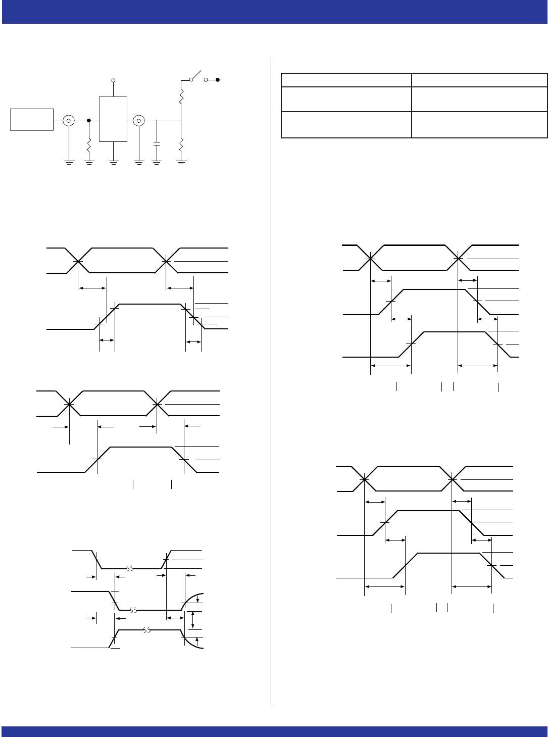
3. See Test Circuits and Waveforms.
4. Minimum limits are guaranteed but not tested on Propagation Delays.
SWITCHING CHARACTERISTICS OVER OPERATING RANGE - MILITARY
(1,2)
FCT805BT FCT805CT
Symbol Parameter Conditions
(3)
Min.
(4)
Max. Min.
(4)
Max. Unit
t
PLH Propagation Delay CL = 50pF 1.5 5.7 1.5 5.2 ns
tPHL INA to OAx, INB to OBx RL = 500Ω
tR Output Rise Time — 2 — 2 ns
tF Output Fall Time — 1.5 — 1.5 ns
t
SK(O) Output skew: skew between outputs of all banks of — 0.9 — 0.7 ns
same package (inputs tied together)
t
SK(P) Pulse skew: skew between opposite transitions — 0.9 — 0.8 ns
of same output (|tPHL -– tPLH|)
t
SK(PP) Part-to-part skew: skew between outputs of different — 1.5 — 1.2 ns
packages at same power supply voltage,
temperature, package type and speed grade
t
PZL Output Enable Time 1.5 6.5 1.5 6 ns
tPZH OEA to OAx, OEB to OBx
t
PLZ Output Disable Time 1.5 6.5 1.5 6 ns
t
PHZ OEA to OAx, OEB to OBx
NOTES:
1. tPLH, tPHL, and tSK(pp) are production tested. All other parameters are guaranteed but not production tested.
2. Propagation delay range indicated by Min. and Max. limit is dues to Vcc, operating temperature, and process parameters. These propagation delay limits do not imply
skew.
3. See Test Circuits and Waveforms.
4. Minimum limits are guaranteed but not tested on Propagation Delays.
SWITCHING CHARACTERISTICS OVER OPERATING RANGE - COMMERCIAL
(1,2)
FCT805BT FCT805CT
Symbol Parameter Conditions
(3)
Min.
(4)
Max. Min.
(4)
Max. Unit
t
PLH Propagation Delay CL = 50pF 1.5 5 1.5 4.5 ns
tPHL INA to OAx, INB to OBx RL = 500Ω
tR Output Rise Time — 1.5 — 1.5 ns
tF Output Fall Time — 1.5 — 1.5 ns
t
SK(O) Output skew: skew between outputs of all banks of — 0.7 — 0.5 ns
same package (inputs tied together)
t
SK(P) Pulse skew: skew between opposite transitions — 0.7 — 0.6 ns
of same output (|tPHL -– tPLH|)
tSK(PP) Part-to-part skew: skew between outputs of different — 1.2 — 1 ns
packages at same power supply voltage,
temperature, package type and speed grade
t
PZL Output Enable Time 1.5 6 1.5 5 ns
tPZH OEA to OAx, OEB to OBx
t
PLZ Output Disable Time 1.5 6 1.5 5 ns
t
PHZ OEA to OAx, OEB to OBx