February 2007 Rev 8 1/16
16
Order codes
Part number Marking Package Packaging
STB75NF75T4 B75NF75 D²PAK Tape & reel
STP75NF75 P75NF75 TO-220 Tube
STP75NF75FP P75NF75 TO-220FP Tube
STB75NF75
STP75NF75 - STP75NF75FP
N-channel 75V - 0.0095 - 80A - TO-220 - TO-220FP - D
2
PA K
STripFET™ II Power MOSFET
General features
Exceptional dv/dt capability
100% avalanche tested
Description
This Power MOSFET series realized with
STMicroelectronics unique STripFET™ process
has specifically been designed to minimize input
capacitance and gate charge. It is therefore
suitable as primary switch in advanced high-
efficiency, high-frequency isolated DC-DC
converters for Telecom and Computer
applications. It is also intended for any
applications with low gate drive requirements.
Applications
Switching application
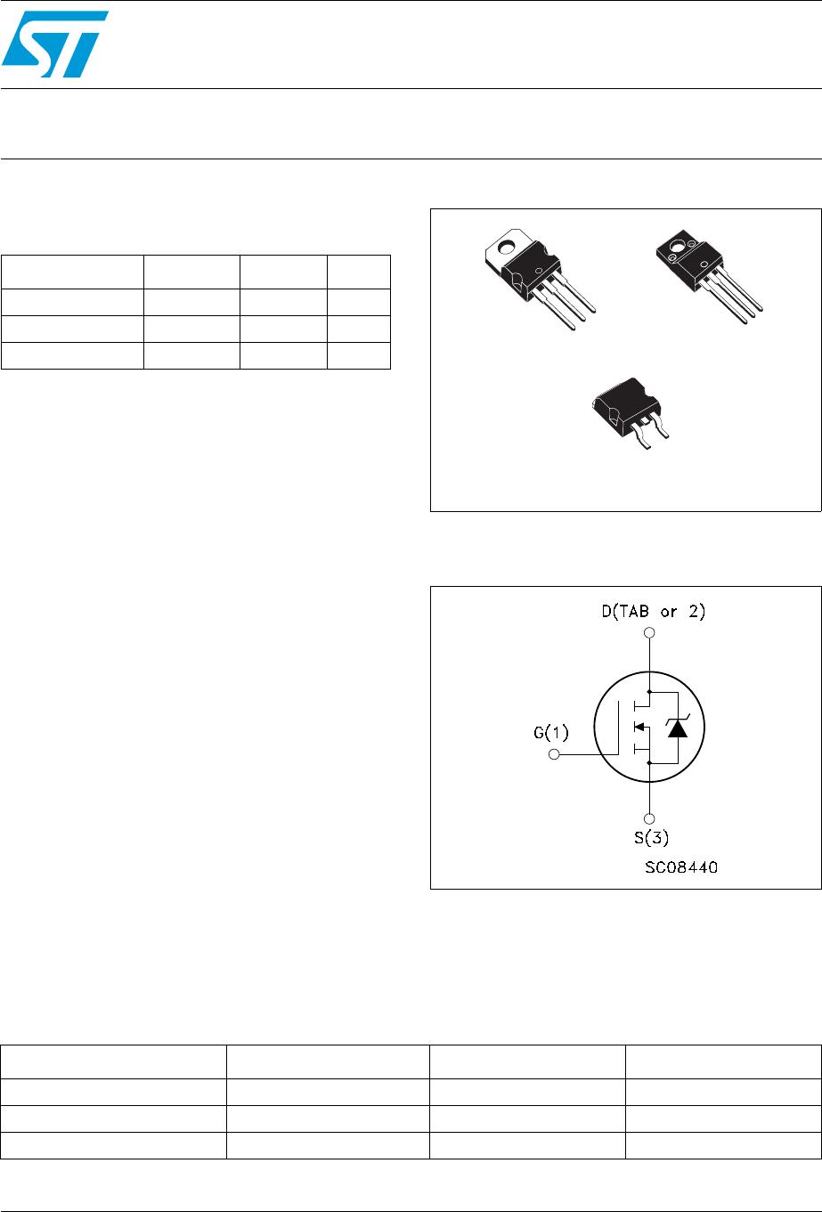
Internal schematic diagram
Type V
DSS
R
DS(on)
I
D
STB75NF75 75V <0.011 80A
(1)
STP75NF75 75V <0.011 80A
(1)
STP75NF75FP 75V <0.011 80A
(1)
1. Current limited by package
1
2
3
TO-220 TO-220FP
D²PAK
1
3
1
2
3
www.st.com
Contents STB75NF75 - STP75NF75 - STP75NF75FP
2/16
Contents
1 Electrical ratings . . . . . . . . . . . . . . . . . . . . . . . . . . . . . . . . . . . . . . . . . . . . 3
2 Electrical characteristics . . . . . . . . . . . . . . . . . . . . . . . . . . . . . . . . . . . . . 4
2.1 Electrical characteristics (curves) . . . . . . . . . . . . . . . . . . . . . . . . . . . . 6
3 Test circuit . . . . . . . . . . . . . . . . . . . . . . . . . . . . . . . . . . . . . . . . . . . . . . . . 9
4 Package mechanical data . . . . . . . . . . . . . . . . . . . . . . . . . . . . . . . . . . . . 10
5 Packaging mechanical data . . . . . . . . . . . . . . . . . . . . . . . . . . . . . . . . . . 14
6 Revision history . . . . . . . . . . . . . . . . . . . . . . . . . . . . . . . . . . . . . . . . . . . 15
STB75NF75 - STP75NF75 - STP75NF75FP Electrical ratings
3/16
1 Electrical ratings
Table 1. Absolute maximum ratings
Symbol Parameter
Value
Unit
D
2
PAK /TO-220 TO-220FP
V
DS
Drain-source voltage (V
GS
= 0) 75 V
V
DGR
Drain-gate voltage (R
GS
= 20K)75V
V
GS
Gate-source voltage ± 20 V
I
D
(1)
1. Current limited by package
Drain current (continuous) at T
C
= 25°C 80 80 A
I
D
(1)
Drain current (continuous) at T
C
=100°C 70
70
A
I
DM
(2)
2. Pulse width limited by safe operating area
Drain current (pulsed) 320
320
A
P
TOT
Total dissipation at T
C
= 25°C 300 45 W
Derating factor 2.0 0.3 W/°C
dv/dt
(3)
3. I
SD
80A, di/dt 300A/µs, V
DD
V
(BR)DSS
, T
j
T
JMAX
Peak diode recovery voltage slope 12 V/ns
E
AS
(4)
4. Starting T
J
= 25
o
C, I
D
= 40A, V
DD
= 37.5V
Single pulse avalanche energy 700 mJ
V
ISO
Insulation withstand voltage (RMS) from all
three leads to external heat sink (t=1s;T
C
=25°C)
-- 2000 V
T
J
T
stg
Operating junction temperature
Storage temperature
-55 to 175 °C
Table 2. Thermal data
Symbol Parameter
Value
Unit
D
2
PAK /TO-220 TO-220FP
R
thJC
Thermal resistance junction-case max 0.5 3.33 °C/W
R
thJA
Thermal resistance junction-ambient max 62.5 °C/W
T
l
Maximum lead temperature for soldering
purpose
(1)
1. 1.6mm from case for 10sec)
300 °C

STP75NF75FP

Mfr. #:
Manufacturer:
STMicroelectronics
Description:
MOSFET N-Ch, 75V-0.0095ohms 80A
Lifecycle:
New from this manufacturer.
Delivery:
DHL FedEx Ups TNT EMS
Payment:
T/T Paypal Visa MoneyGram Western Union

Products related to this Datasheet