AD628
Rev. G | Page 15 of 20
THEORY OF OPERATION
The AD628 is a high common-mode voltage difference
amplifier, combined with a user-configurable output amplifier
(see
Figure 28 and Figure 29). Differential mode voltages in
excess of 120 V are accurately scaled by a precision 11:1 voltage
divider at the input. A reference voltage input is available to the
user at Pin 3 (V
REF
). The output common-mode voltage of the
difference amplifier is the same as the voltage applied to the
reference pin. If the uncommitted amplifier is configured for
gain, connect Pin 3 to one end of the external gain resistor to
establish the output common-mode voltage at Pin 5 (OUT).
The output of the difference amplifier is internally connected to
a 10 kΩ resistor trimmed to better than ±0.1% absolute accuracy.
The resistor is connected to the noninverting input of the
output amplifier and is accessible at Pin 4 (C
FILT
). A capacitor
can be connected to implement a low-pass filter, a resistor can
be connected to further reduce the output voltage, or a clamp
circuit can be connected to limit the output swing.
The uncommitted amplifier is a high open-loop gain, low offset,
low drift op amp, with its noninverting input connected to the
internal 10 kΩ resistor. Both inputs are accessible to the user.
Careful layout design has resulted in exceptional common-
mode rejection at higher frequencies. The inputs are connected
to Pin 1 (+IN) and Pin 8 (−IN), which are adjacent to the power
pins, Pin 2 (−V
S
) and Pin 7 (+V
S
). Because the power pins are at
ac ground, input impedance balance and, therefore, common-
mode rejection are preserved at higher frequencies.
+IN
–IN
+IN
–IN
A2
A1
+IN
–IN
100k
100k
10k
10k
V
REF
10k
OUT
G = +0.1
C
FILT
R
G
02992-028
5
6
43
1
8
Figure 28. Simplified Schematic
+V
S
+IN
–IN
–V
S
A2
+IN
–IN
100k
100k
10k
10k
V
REF
REFERENCE
VOLTAGE
10k
AD628
OUT
G = +0.1
R
G
R
EXT3
C
FILT
R
EXT2
R
EXT1
+IN
–IN
A1
5
32
1
8
6
02992-029
47
Figure 29. Circuit Connections
AD628
Rev. G | Page 16 of 20
APPLICATIONS INFORMATION
GAIN ADJUSTMENT
The AD628 system gain is provided by an architecture
consisting of two amplifiers (see
Figure 29). The gain of the
input stage is fixed at 0.1; the output buffer is user adjustable
as G
A2
= 1 + R
EXT1
/R
EXT2
. The system gain is then
+×=
EXT2
EXT1
TOTAL
R
R
G 10.1
(1)
At a 2 nA maximum, the input bias current of the buffer amplifier
is very low and any offset voltage induced at the buffer amplifier
by its bias current may be neglected (2 nA × 10 kΩ = 20 µV).
However, to absolutely minimize bias current effects, select
R
EXT1
and R
EXT2
so that their parallel combination is 10 kΩ. If
practical resistor values force the parallel combination of R
EXT1
and R
EXT2
below 10 kΩ, add a series resistor (R
EXT3
) to make up
for the difference.
Table 5 lists several values of gain and
corresponding resistor values.
Table 5. Nearest Standard 1% Resistor Values for
Various Gains (see
Figure 29)
Total Gain
(V/V)
A2 Gain
(V/V)
R
EXT1
(Ω) R
EXT2
(Ω) R
EXT3
(Ω)
0.1 1 10 k 0
0.2 2 20 k 20 k 0
0.25 2.5 25.9 k 18.7 k 0
0.5 5 49.9 k 12.4 k 0
1 10 100 k 11 k 0
2 20 200 k 10.5 k 0
5 50 499 k 10.2 k 0
10 100 1 M 10.2 k 0
To set the system gain to <0.1, create an attenuator by placing
Resistor R
EXT4
from Pin 4 (C
FILT
) to the reference voltage. A
divider is formed by the 10 kΩ resistor that is in series with the
positive input of A2 and Resistor R
EXT4
. A2 is configured for
unity gain.
Using a divider and setting A2 to unity gain yields
1
k10
0.1
/
×
+
×=
EXT4
EXT4
DIVIDERW
R
R
G
INPUT VOLTAGE RANGE
VREF and the supply voltage determine the common-mode
input voltage range. The relation is expressed by
REF
SCM
VVV
UPPER
10)V2.1(11
+
(2)
REF
SCM
VV 10)V2.1(11V
LOWER
+
where:
V
S+
is the positive supply.
V
S−
is the negative supply.
1.2 V is the headroom needed for suitable performance.
Equation 2 provides a general formula for calculating the
common-mode input voltage range. However, keep the AD628
within the maximum limits listed in
Tabl e 1 to maintain
optimal performance. This is illustrated in
Figure 30 where the
maximum common-mode input voltage is limited to ±120 V.
Figure 31 shows the common-mode input voltage bounds for
single-supply voltages.
–200
–150
–100
–50
0
50
INPUT COMMON-MODE VOLTAGE (V)
100
150
200
862401012
SUPPLY VOLTAGE (±V)
02992-035
1416
MAXIMUM INPUT COMMON-MODE
VOLTAGE WHEN V
REF
= GND
Figure 30. Input Common-Mode Voltage vs. Supply Voltage
for Dual Supplies
–80
–60
–40
–20
0
20
40
60
80
100
INPUT COMMON-MODE VOLTAGE (V)
862401012
SINGLE-SUPPLY VOLTAGE (V)
02992-034
1416
MAXIMUM INPUT COMMON-MODE
VOLTAGE WHEN V
REF
= MIDSUPPLY
Figure 31. Input Common-Mode Voltage vs.
Supply Voltage for Single Supplies
AD628
Rev. G | Page 17 of 20
The differential input voltage range is constrained to the linear
operation of the internal amplifiers, A1 and A2. The voltage
applied to the inputs of A1 and A2 should be between
V
S−
+ 1.2 V and V
S+
− 1.2 V. Similarly, the outputs of A1 and A2
should be kept between V
S−
+ 0.9 V and V
S+
− 0.9 V.
VOLTAGE LEVEL CONVERSION
Industrial signal conditioning and control applications typically
require connections between remote sensors or amplifiers and
centrally located control modules. Signal conditioners provide
output voltages of up to ±10 V full scale. However, ADCs or
microprocessors operating on single 3.3 V to 5 V logic supplies
are now the norm. Thus, the controller voltages require further
reduction in amplitude and reference.
Furthermore, voltage potentials between locations are seldom
compatible, and power line peaks and surges can generate
destructive energy between utility grids. The AD628 offers an
ideal solution to both problems. It attenuates otherwise destruc-
tive signal voltage peaks and surges by a factor of 10 and shifts
the differential input signal to the desired output voltage.
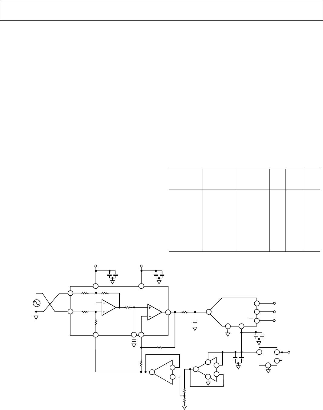
Conversion from voltage-driven or current-loop systems is
easily accomplished using the circuit shown in
Figure 32. This
shows a circuit for converting inputs of various polarities and
amplitudes to the input of a single-supply ADC.
To adjust common-mode output voltage, connect Pin 3 (V
REF
)
and the lower end of the 10 kΩ resistor to the desired voltage.
The output common-mode voltage is the same as the reference
voltage.
Designing such an application can be done in a few simple
steps, which includes the following:
Determine the required gain. For example, if the input
voltage must be changed from ±10 V to +5 V, the gain now
needs to be +5/+20 or +0.25.
Determine if the circuit common-mode voltage should be
changed. An
AD7940 ADC is illustrated for this example.
When operating from a 5 V supply, the common-mode
voltage of the
AD7940 is half the supply, or 2.5 V. If the
AD628 reference pin and the lower terminal of the 10 kΩ
resistor are connected to a 2.5 V voltage source, the output
common-mode voltage is 2.5 V.
Table 6 shows resistor and reference values for commonly used
single-supply converter voltages. R
EXT3
is included as an option
to balance the source impedance into A2. This is described in
more detail in the
Gain Adjustment section.
Table 6. Nearest 1% Resistor Values for Voltage Level
Conversion Applications
Input
Voltage (V)
ADC
Supply
Voltage (V)
Desired
Output
Voltage (V)
V
REF
(V)
R
EXT1
(kΩ)
R
EXT2
kΩ)
±10 5 2.5 2.5 15 10
±5 5 2.5 2.5 39.7 10
+10 5 2.5 0 39.7 10
+5 5 2.5 0 89.8 10
±10 3 1.25 1.25 2.49 10
±5 3 1.25 1.25 15 10
+10 3 1.25 0 15 10
+5 3 1.25 0 39.7 10
5
1
3 4
8
2
7
+V
S
–V
S
6
–IN
+IN
V
REF
100k
10k
100k
10k
10k
A1
A2
4
5
6
3
1
2
SCLK
SDATA
CS
GND
V
DD
V
IN
AD628
SERIAL DATA
REF195
+12V
V
OUT
V
IN
2
3
4
6
C
FILT
R
G
10F
0.1F
10F
0.1F
10F0.1F 10F0.1F
AD7940
±10V
15nF
2
3
1
AD8606
1/2
49.9
33nF
+12
V
12
V
10k
10k
AD628 REFERENCE VO LTAGE
R
EXT2
10k
R
E
X
T
1
1
5
k
AD8606
2/2
5
6
7
4
8
02992-030
OUT
Figure 32. Level Shifter

AD628ARZ

Mfr. #:
Manufacturer:
Analog Devices Inc.
Description:
Differential Amplifiers Hi CM Vltg Gain Prog
Lifecycle:
New from this manufacturer.
Delivery:
DHL FedEx Ups TNT EMS
Payment:
T/T Paypal Visa MoneyGram Western Union