12
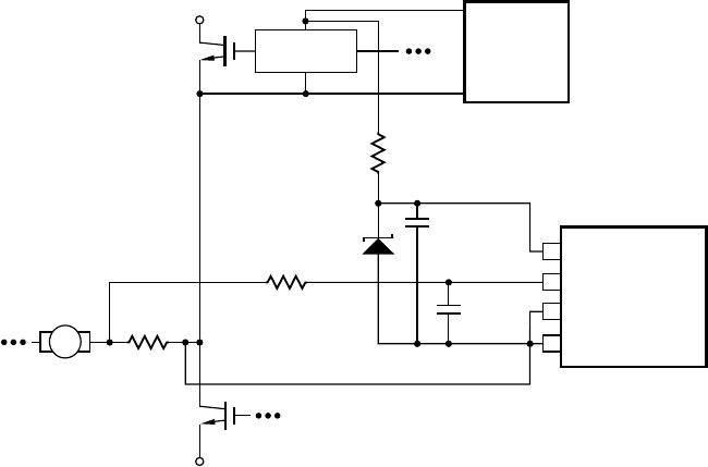
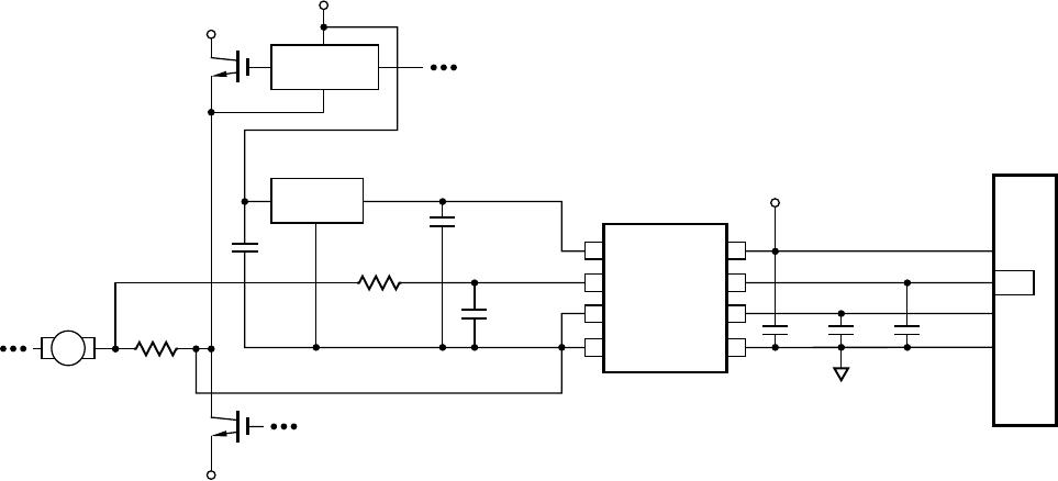
Figure 17. Recommended HCPL-7520 application circuit.
As shown in Figure 17, 0.1 µF bypass capacitors (C1, C2)
should be located as close as possible to the pins of the
HCPL-7520. The bypass capacitors are required because
of the high-speed digital nature of the signals inside the
HCPL-7520. A 0.01 µF bypass capacitor (C2) is also rec-
ommended at the input due to the switched-capacitor
nature of the input circuit. The input bypass capacitor
also forms part of the anti-aliasing lter, which is recom-
mended to prevent high frequency noise from aliasing
down to lower frequencies and interfering with the
input signal. The input lter also performs an important
reliability function—it reduces transient spikes from ESD
events owing through the current sensing resistor.
PC Board Layout
The design of the printed circuit board (PCB) should
follow good layout practices, such as keeping bypass
capacitors close to the supply pins, keeping output
signals away from input signals, the use of ground and
power planes, etc. In addition, the layout of the PCB
can also aect the isolation transient immunity (CMTI)
of the HCPL-7520, due primarily to stray capacitive
coupling between the input and the output circuits. To
obtain optimal CMTI performance, the layout of the PC
board should minimize any stray coupling by maintain-
ing the maximum possible distance between the input
and output sides of the circuit and ensuring that any
ground or power plane on the PC board does not pass
directly below or extend much wider than the body of
the HCPL-7520.
+
-
MOTOR
HV-
HV+
R
SENSE
FLOATING
POSITIVE
SUPPLY
GATE DRIVE
CIRCUIT
HCPL-7520
C2
0.1 µF
C3
0.01 µF
R5
68 Ω
R1
1
2
3
4
8
7
6
5
IN OUT
C1
0.1 µF
U1
78L05
C4 C5 C6
V
DD1
V
IN+
V
IN-
GND1
V
DD2
V
OUT
V
REF
GND2
A/D
V
REF
GND
µC
C6 = 150 pF
C4 = C5 = 0.1 µF
+5 V