ADG438F/ADG439F
Rev. E | Page 12 of 16
TERMINOLOGY
V
DD
Most positive power supply potential.
V
SS
Most negative power supply potential.
GND
Ground (0 V) reference.
R
ON
Ohmic resistance between D and S.
ΔR
ON
ΔR
ON
represents the difference between the R
ON
of any two
channels as a percentage of the maximum R
ON
of those two
channels.
R
FLAT (ON)
Flatness is defined as the difference between the maximum and
minimum value of the on resistance measured over the specified
analog signal range and is represented by R
FLAT (ON)
.
Flatness is calculated by
((R
MAX
− R
MIN
) / R
MAX
× 100)
R
ON
Drift
Change in R
ON
when temperature changes by one degree Celsius.
I
S
(Off)
Source leakage current when the switch is off.
I
D
(Off)
Drain leakage current when the switch is off.
I
D
, I
S
(On)
Channel leakage current when the switch is on.
V
D
(V
S
)
Analog voltage on Terminal D and Terminal S.
I
S
(Fault—Power Supplies On)
Source leakage current when exposed to an overvoltage
condition.
I
D
(Fault—Power Supplies On)
Drain leakage current when exposed to an overvoltage
condition.
I
S
(Fault—Power Supplies Off)
Source leakage current with power supplies off.
C
S
(Off)
Channel input capacitance for off condition.
C
D
(Off)
Channel output capacitance for off condition.
C
D
, C
S
(On)
On switch capacitance.
C
IN
Digital input capacitance.
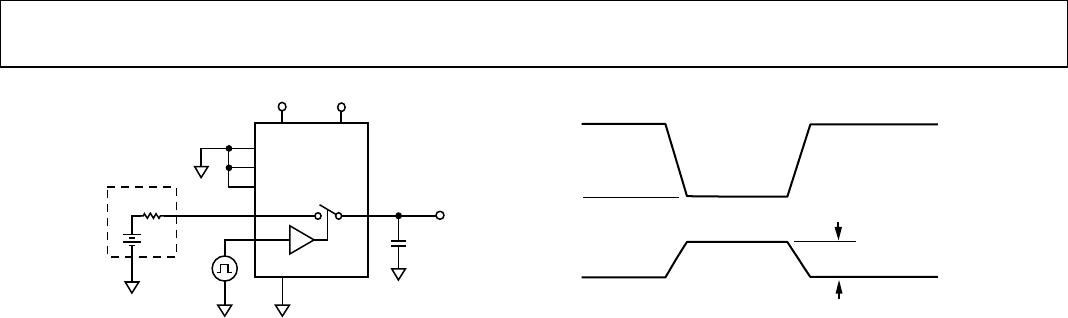
t
ON
(EN)
Delay time between the 50% and 90% points of the digital input
and switch on condition.
t
OFF
(EN)
Delay time between the 50% and 90% points of the digital input
and switch off condition.
t
TRANSITION
Delay time between the 50% and 90% points of the digital
inputs and the switch on condition when switching from one
address state to another.
t
OPEN
Off time measured between 80% points of both switches when
switching from one address state to another.
V
INL
Maximum input voltage for Logic 0.
V
INH
Minimum input voltage for Logic 1.
I
INL
(I
INH
)
Input current of the digital input.
Off Isolation
A measure of unwanted signal coupling through an off channel.
Charge Injection
A measure of the glitch impulse transferred from the digital
input to the analog output during switching.
I
DD
Positive supply current.
I
SS
Negative supply current.