SI1023X-T1-GE3

www.vishay.com
4
Document Number: 71169
S10-2432-Rev. C, 25-Oct-10
Vishay Siliconix
Si1023X
TYPICAL CHARACTERISTICS (T
A
= 25 °C, unless otherwise noted)
Vishay Siliconix maintains worldwide manufacturing capability. Products may be manufactured at one of several qualified locations. Reliability data for Silicon
Technology and Package Reliability represent a composite of all qualified locations. For related documents such as package/tape drawings, part marking, and
reliability data, see www.vishay.com/ppg?71169
.
Threshold Voltage Variance vs. Temperature
- 0.3
- 0.2
- 0.1
0.0
0.1
0.2
0.3
- 50 - 25 0 25 50 75 100 125
I
D
= 0.25 mA
Variance (V)V
GS(th)
T
J
- Temperature (°C)
I
GSS
vs. Temperature
0.0
0.5
1.0
1.5
2.0
2.5
3.0
- 50 - 25 0 25 50 75 100 125
T
J
-Temperature (°C)
I
GSS
- (µA)
V
GS
= 4.5 V
BV
GSS
vs. Temperature
0
1
2
3
4
5
6
7
- 50 - 25 0 25 50 75 100 125
T
J
- Temperature (°C)
BV
GSS
- Gate-to-Source Breakdown Voltage (V)
Normalized Thermal Transient Impedance, Junction-to-Ambient
10
-3
10
-2
00601110
-1
10
-4
100
2
1
0.1
0.01
0.2
0.1
0.05
0.02
Single Pulse
Duty Cycle = 0.5
Square Wave Pulse Duration (s)
Normalized Effective Transient
Thermal Impedance
1. Duty Cycle, D =
2. Per Unit Base = R
thJA
= 500 °C/W
3. T
JM
- T
A
= P
DM
Z
thJA
(t)
t
1
t
2
t
1
t
2
Notes:
4. Surface Mounted
P
DM
Package Information
www.vishay.com
Vishay Siliconix
Revision: 11-Aug-14
1
Document Number: 71612
For technical questions, contact: analogswitchtechsupport@vishay.com
THIS DOCUMENT IS SUBJECT TO CHANGE WITHOUT NOTICE. THE PRODUCTS DESCRIBED HEREIN AND THIS DOCUMENT
ARE SUBJECT TO SPECIFIC DISCLAIMERS, SET FORTH AT www.vishay.com/doc?91000
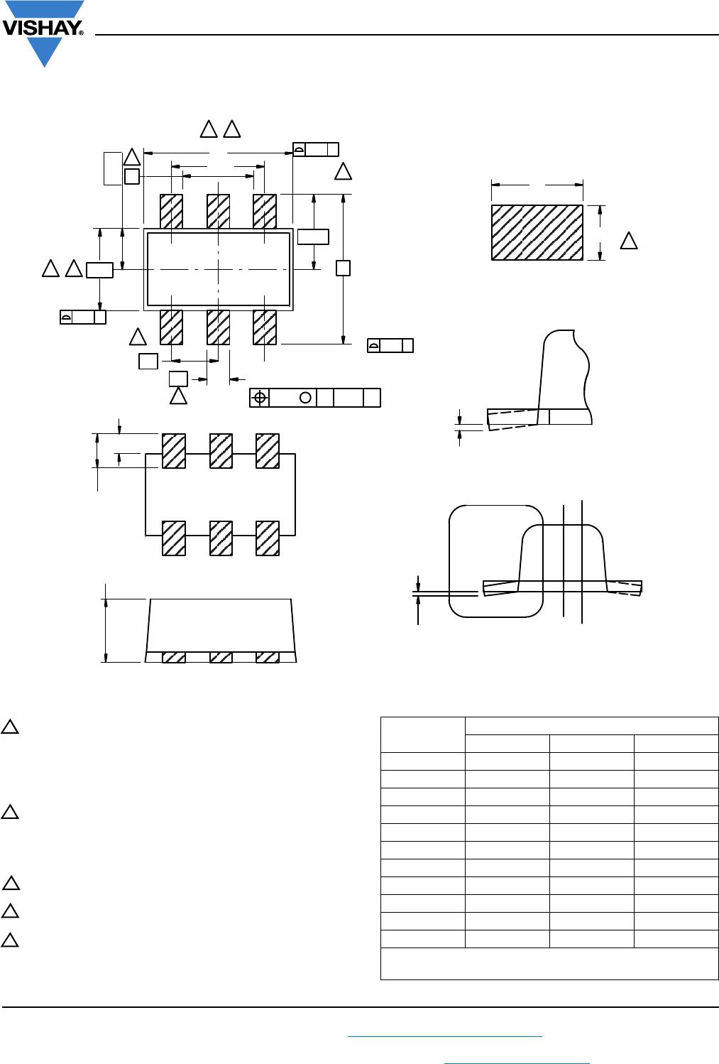
SC-89 6-Leads (SOT-563F)
Notes
1. Dimensions in millimeters.
2. Dimension D does not include mold flash, protrusions or gate
burrs. Mold flush, protrusions or gate burrs shall not exceed
0.15 mm per dimension E1 does not include interlead flash
or protrusion, interlead flash or protrusion shall not exceed
0.15 mm per side.
3. Dimensions D and E1 are determined at the outmost extremes
of the plastic body exclusive of mold flash, the bar burrs, gate
burrs and interlead flash, but including any mismatch between
the top and the bottom of the plastic body.
4. Datums A, B and D to be determined 0.10 mm from the lead tip.
5. Terminal numbers are shown for reference only.
6. These dimensions apply to the flat section of the lead between
0.08 mm and 0.15 mm from the lead tip.
6
4
32
4
32
5
4
Caaa
C
M
ddd
A–B D
2x
e
B
6x b
Caaa
2x
D
E/2
E
Cbbb
2x
123
654
E1
E1/2
A
D
e1
L1
L
A
B
C
A1
A1
SECTION B-B
DETAIL “A”
SEE DETAIL “A”
DIM.
MILLIMETERS
MIN. NOM. MAX.
A 0.56 0.58 0.60
A1 0 0.02 0.10
b 0.15 0.22 0.30
c 0.10 0.14 0.18
D 1.50 1.60 1.70
E 1.50 1.60 1.70
E1 1.15 1.20 1.25
e 0.45 0.50 0.55
e1 0.95 1.00 1.05
L 0.25 0.35 0.50
L1 0.10 0.20 0.30
C14-0439-Rev. C, 11-Aug-14
DWG: 5880
Application Note 826
Vishay Siliconix
Document Number: 72605 www.vishay.com
Revision: 21-Jan-08 21
APPLICATION NOTE
RECOMMENDED MINIMUM PADS FOR SC-89: 6-Lead
0.051
(1.300)
0.069
(1.753)
0.019
(0.478)
0.031
(0.798)
0.012
(0.300)
0.051
(0.201)
0.020
(0.500)
Recommended Minimum Pads
Dimensions in Inches/(mm)
Return to Index
Return to Index

SI1023X-T1-GE3

Mfr. #:
Manufacturer:
Vishay / Siliconix
Description:
MOSFET Dual P-Ch MOSFET 20V 1.2 ohms @ 4.5V
Lifecycle:
New from this manufacturer.
Delivery:
DHL FedEx Ups TNT EMS
Payment:
T/T Paypal Visa MoneyGram Western Union

Products related to this Datasheet