ISL9307
5
FN7931.3
September 20, 2012
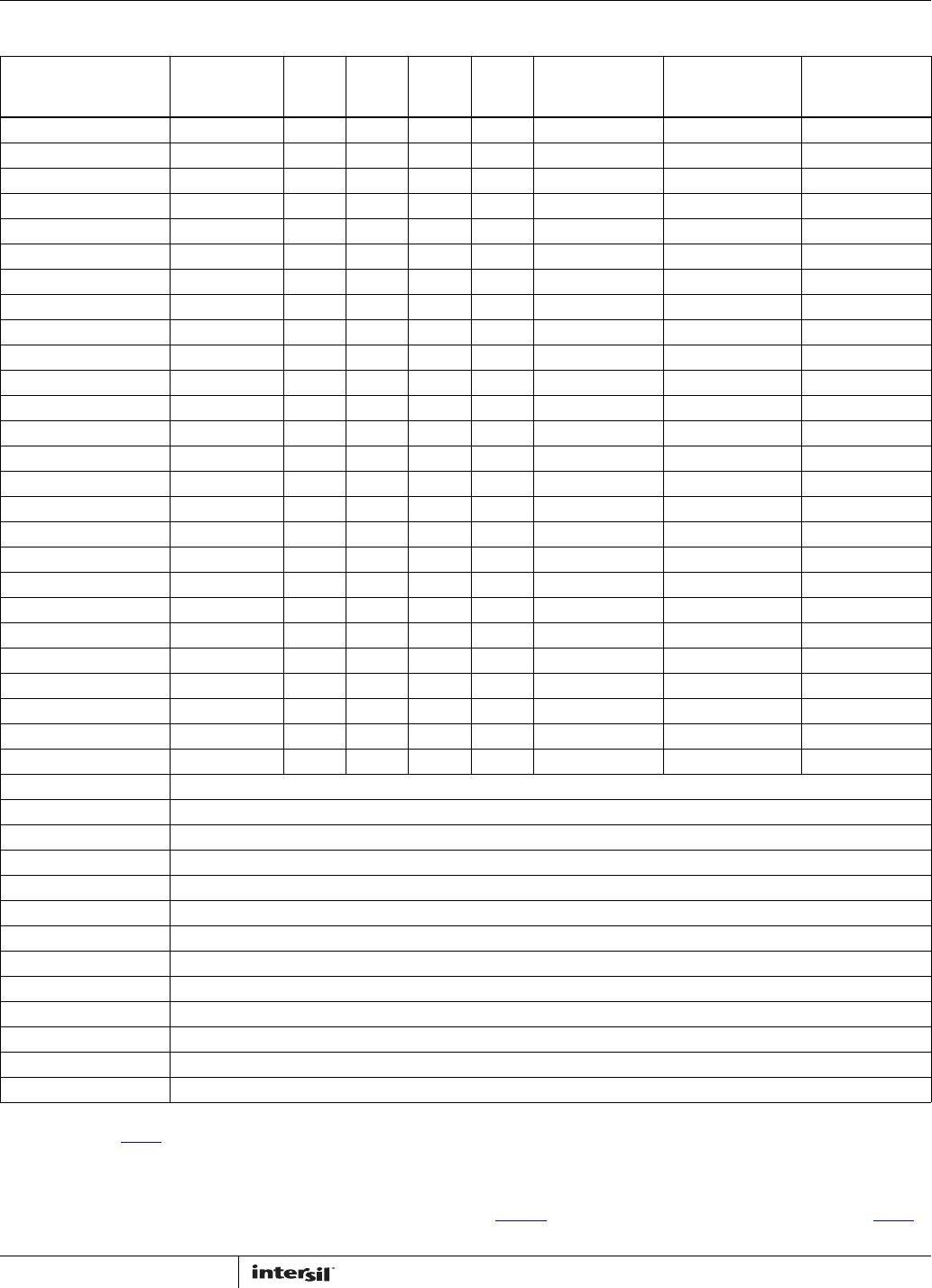
Absolute Maximum Ratings (Refer to Ground) Thermal Information
SW1, SW2 . . . . . . . . . . . . . . . . . . . . . . . . . . . . . . . . . . . . . . . . . . -1.5V to 6.5V
FB1, FB2 . . . . . . . . . . . . . . . . . . . . . . . . . . . . . . . . . . . . . . . . . . . -0.3V to 3.6V
GNDDCD1, GNDDCD2, GNDLDO. . . . . . . . . . . . . . . . . . . . . . . . -0.3V to 0.3V
All other pins . . . . . . . . . . . . . . . . . . . . . . . . . . . . . . . . . . . . . . . . -0.3V to 6.5V
ESD Ratings
Human Body Model (Tested per JESD22-A114F) . . . . . . . . . . . . . . .3.5kV
Machine Model (Tested per JESD22-A115-A) . . . . . . . . . . . . . . . . . 225V
Charged Device Model (Tested per JESD22-C101D) . . . . . . . . . . . .2.2kV
Latch Up (Tested per JESD78B, Class II, Level A) . . . . . . . . . . . . . . . 100mA
Thermal Resistance (Typical) θ
JA
(°C/W)
16 Ld TQFN Package (Note 4). . . . . . . . . . . . . . . . . . . . . 40.2
Maximum Junction Temperature Range . . . . . . . . . . . . . .-40°C to +150°C
Recommended Junction Temperature Range . . . . . . . . .-40°C to +125°C
Storage Temperature Range. . . . . . . . . . . . . . . . . . . . . . . .-65°C to +150°C
Recommended Operating Conditions
VINDCD1 . . . . . . . . . . . . . . . . . . . . . . . . . . . . . . . . . . . . . . . . . . . . 2.5V to 5.5V
VINDCD2 . . . . . . . . . . . . . . . . . . . . . . . . . . . . . . . . . . . . . . . . 2.3V to VINDCD1
VINLDO. . . . . . . . . . . . . . . . . . . . . . . . . . . . . . . . . . . . . . . . . . 1.5V to VINDCD1
DCD1 and DCD2 Output Current . . . . . . . . . . . . . . . . . . . . 0mA to 1500mA
LDO1 and LDO2 Output Current . . . . . . . . . . . . . . . . . . . . . . 0mA to 300mA
Operating Ambient Temperature . . . . . . . . . . . . . . . . . . . . . -40
°
C to +85
°
C
CAUTION: Do not operate at or near the maximum ratings listed for extended periods of time. Exposure to such conditions may adversely impact product
reliability and result in failures not covered by warranty.
NOTE:
4. θ
JA
is measured in free air with the component mounted on a high effective thermal conductivity test board with “direct attach” features. See Tech
Brief TB379
.
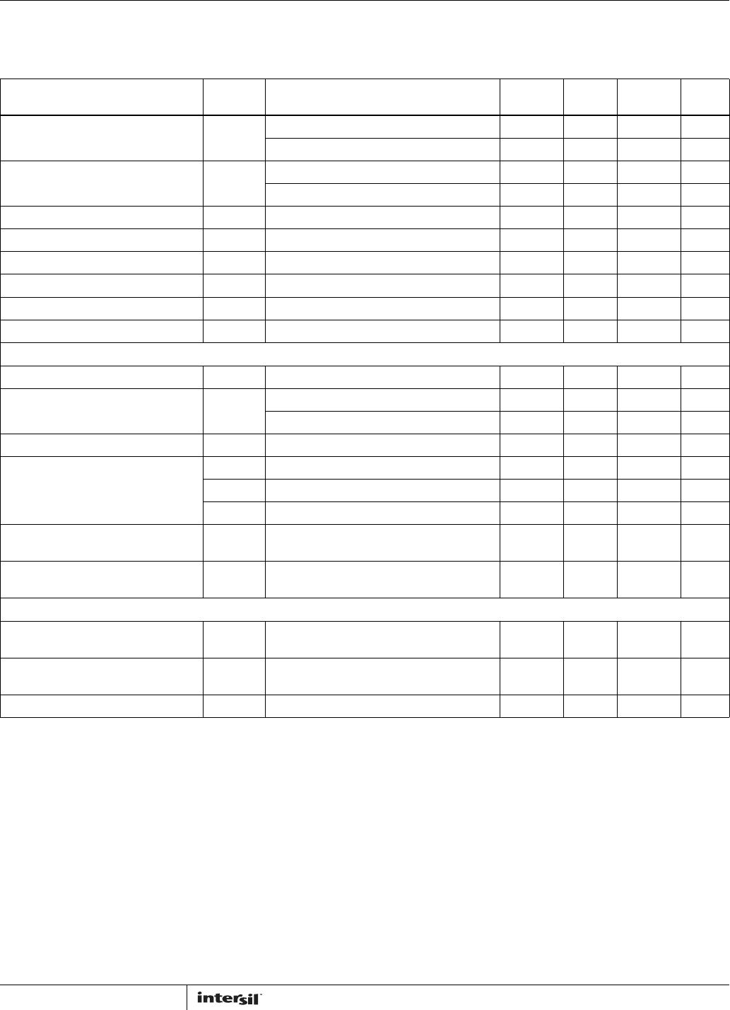
Electrical Specifications Unless otherwise noted, typical specifications are measured at the following conditions: T
A
= +25°C,
VINDCD1 = 3.6V, VINDCD2 = 3.3V. For LDO1 and LDO2, VINLDO = VOLDO + 0.5V to 5.5V with VINLDO always no higher than VINDCD1.
L
1
=L
2
= 1.5µH, C
1
= C
4
= C
5
= 10µF, C
2
= C
6
= C
7
= 1µF, I
OUT
= 0A for DCD1, DCD2, LDO1 and LDO2 (seeFigure 1 on page 1 for more details).
Boldface limits apply over the operating temperature range, -40°C to +85°C.
PARAMETER SYMBOL TEST CONDITIONS
MIN
(Note 5) TYP
MAX
(Note 5) UNIT
VINDCD1, VINDCD2 Voltage Range 2.5 - 5.5 V
VINDCD1, VINDCD2 Undervoltage
Lockout Threshold
V
UVLO
Rising - 2.2 2.3 V
Falling 1.9 2.1 - V
Quiescent Supply Current on VINDCD1 I
VIN1
Only DCD1 enabled; no load and no switching
on DCD1
-4060 µA
I
VIN2
Only DCD1 and LDO1 enabled; no load and no
switching on DCD1
-6095 µA
I
VIN3
Both DCD1 and DCD2 enabled; no load and no
switching on both DCD1 and DCD2
-5075 µA
I
VIN4
Only LDO1 and LDO2 enabled - 110 130 µA
I
VIN5
DCD1, DCD2, LDO1 and LDO2 enabled; no load
and no switching on both DCD1 and DCD2
-135160 µA
Shutdown Supply Current I
SD
VINDCD1 = 5.5V; DCD1, DCD2, LDO1 and LDO2
disabled
-0.155 µA
Thermal Shutdown - 155 - °C
Thermal Shutdown Hysteresis -30-°C
DCD1 AND DCD2
FB1, FB2 Regulation Voltage V
FB
0.785 0.8 0.815 V
FB1, FB2 Bias Current I
FB
FB = 0.75V - 0.001 - µA
Output Voltage Accuracy V
IN
= V
O
+ 0.5V to 5.5V (minimal 2.5V), 1mA
load
-3 - +3 %
Line Regulation V
IN
= V
O
+ 0.5V to 5.5V (minimal 2.5V) - 0.1 - %/V
Maximum Output Current 1500 --mA