Rev 03 Jan 2013 19:42 | Page 3
Note that the electrode interfaces +VIN, -VIN and RLD are equipped with 180kΩ and 499kΩ (R6,
R7 and R1 respectively) resistors to limit current injection to the subject in the event of fault or
overload. Please note that these will not protect against supply line transients coming through
the system. Isolation from the power line is always required when connecting to a live subject. It
is recommended to fully understand common safety practices; the proper application of such
guidelines is sole responsibility of the end user.
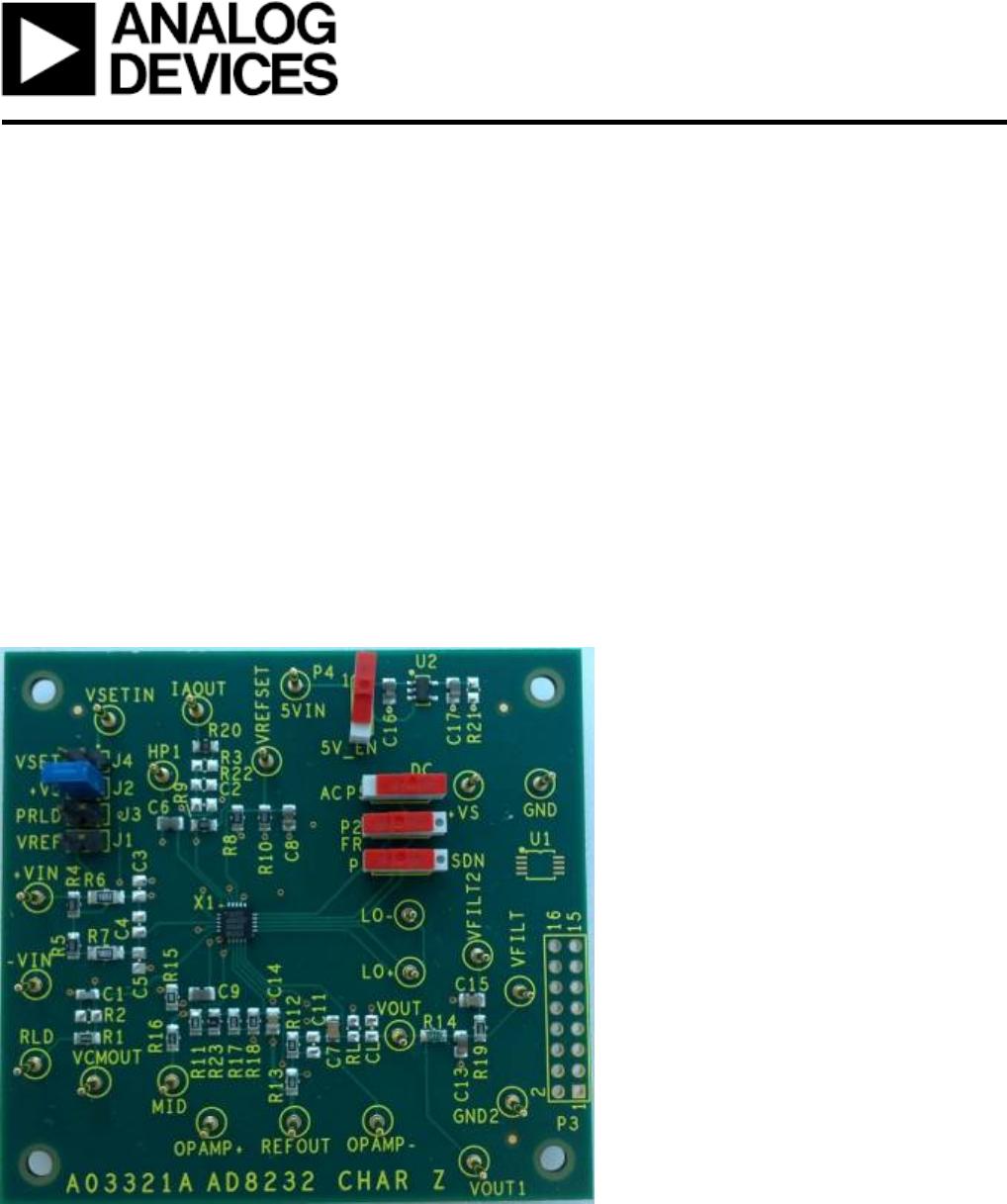
DEFAULT CIRCUIT CONFIGURATION
Signal Path: Inamp and Filters
The evaluation board ships with a default configuration for applications that involve three-electrodes
connected at the hands. The terminals +VIN, –VIN, and RLD serve as the inputs and right-leg drive
electrode connections respectively.
The instrumentation amplifier has a fixed gain of 100 and the op-amp is set for a gain of 11. The
overall gain is 1100V/V, which limits the maximum differential input signal to about 2.7mVp-p.
Exceeding this amplitude will not damage the AD8232, but the signal at the output will appear
distorted. Due to the filter’s high-Q, there is additional peaking that sets the maximum observed gain
above 1100V/V around 15Hz. The total gain may be changed by adjusting the resistors R12 and R13,
but this will have a direct impact on the Q of the low-pass filter. Note that the instrumentation
amplifier has a fixed gain of 100.
A single-supply is used to implement the entire signal chain. For this purpose, the reference buffer is
set to a ratiometric level at mid-supply using two 10MΩ resistors (R8 and R10). The integrated
reference buffer output provides a virtual ground level to allow high-pass filtering. The signal at the
output will ride on top of this mid-supply level. This voltage is available at the REFOUT pin to serve as
a zero level for subsequent signal-acquisition stages.
The circuit implements a two-pole high pass filter for eliminating motion artifacts and the electrode
half-cell potential. Additionally, the integrated operational amplifier creates a two-pole low pass filter
to remove line noise and other interference signals. The frequency cutoff of all filters may be changed
by adjusting component values.
A complete version of the schematic and a section summarizing the explanation of the components
can be found at the end of this document.