©2005 Fairchild Semiconductor Corporation 1 www.fairchildsemi.com
MMBT5550 Rev. A
MMBT5550 NPN General Purpose Amplifier
August 2005
MMBT5550
NPN General Purpose Amplifier
• This device is designed for general purpose high voltage amplifiers
and gas discharge display drivers.
Absolute Maximum Ratings * T
a
= 25°C unless otherwise noted
* These ratings are limiting values above which the serviceability of any semiconductor device may be impaired.
NOTES:
1. These ratings are based on a maximum junction temperature of 150 degrees C.
2. These are steady state limits. The factory should be consulted on applications involving pulsed or low duty cycle operations.
Electrical Characteristics T
a
= 25°C unless otherwise noted
Symbol Parameter Value Units
V
CEO
Collector-Emitter Voltage 140 V
V
CBO
Collector-Base Voltage 160 V
V
EBO
Emitter-Base Voltage 6.0 V
I
C
Collector current - Continuous 600 mA
T
J
, T
stg
Junction and Storage Temperature -55 ~ +150 °C
Symbol Parameter Test Condition Min. Max. Units
Off Characteristics
V
(BR)CEO
Collector-Emitter Breakdown Voltage * I
C
= 1.0mA, I
B
= 0 140 V
V
(BR)CBO
Collector-Base Breakdown Voltage I
C
= 100µA, I
E
= 0 160 V
V
(BR)EBO
Emitter-Base Breakdown Voltage I
E
= 10mA, I
C
= 0 6.0 V
I
CBO
Collector Cutoff Current V
CB
= 100V, I
E
= 0
V
CB
= 100V, I
E
= 0, T
a
= 100°C
100
100
nA
µA
I
EBO
Emitter Cutoff Current V
EB
= 4.0V, I
C
= 0 50 nA
On Characteristics
h
FE
DC Current Gain I
C
= 1.0mA, V
CE
= 5.0V
I
C
= 10mA, V
CE
= 5.0V
I
C
= 50mA, V
CE
= 5.0V
60
60
20
250
V
CE(sat)
Collector-Emitter Saturation Voltage I
C
= 10mA, I
B
= 1.0mA
I
C
= 50mA, I
B
= 5.0mA
0.15
0.25
V
V
V
BE(sat)
Base-Emitter On Voltage I
C
= 10mA, I
B
= 1.0mA
I
C
= 50mA, I
B
= 5.0mA
1.0
1.2
V
V
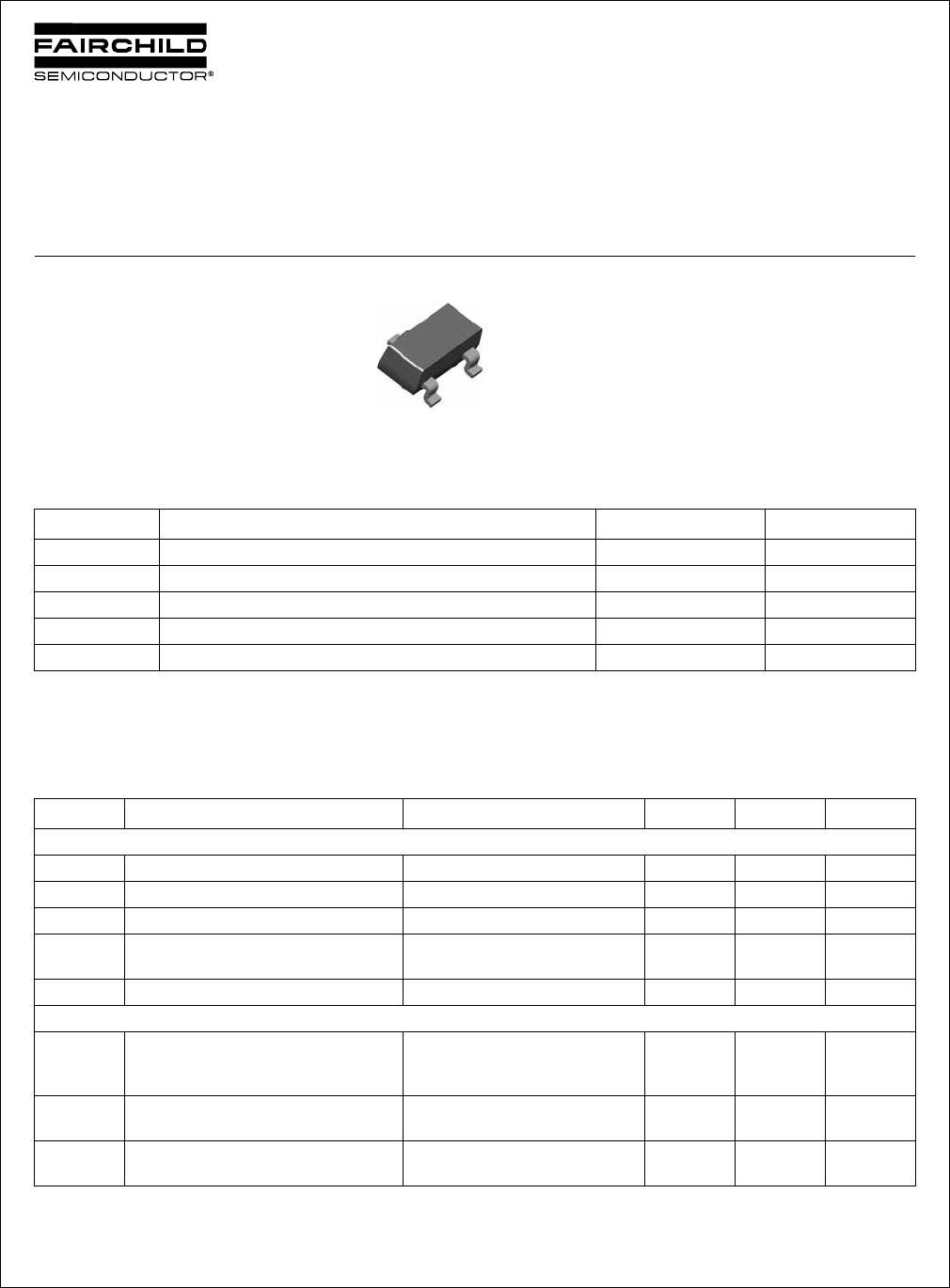
SOT-23
1. Base 2. Emitter 3. Collector
1
2
3
Marking: 1F