ATF16LV8C
4
Notes: 1. Output data is latched and held.
2. High-Z outputs remain High-Z.
3. Clock and input transitions are ignored.
AC Characteristics
Symbol Parameter
-10 -15
UnitsMin Max Min Max
t
PD
Input or Feedback to Non-Registered Output 1 10 1 15 ns
t
CF
Clock to Feedback 5 8 ns
t
CO
Clock to Output 2 7 2 10 ns
t
S
Input or Feedback Setup Time 7 12 ns
t
H
Input Hold Time 0 0 ns
t
P
Clock Period 12 16 ns
t
W
Clock Width 6 8 ns
f
MAX
External Feedback 1/(t
S
+ t
CO
) 71.4 45.5 MHz
Internal Feedback 1/(t
S
+ t
CF
) 83.3 50 MHz
No Feedback 1/(t
P
) 83.3 62.5 MHz
t
EA
Input to Output Enable — Product Term 3 10 3 15 ns
t
ER
Input to Output Disable — Product Term 2 10 2 15 ns
t
PZX
OE pin to Output Enable 2 8 2 15 ns
t
PXZ
OE pin to Output Disable 1.5 8 1.5 15 ns
Power-down AC Characteristics
(1)(2)(3)
Symbol Parameter
-10 -15
UnitsMin Max Min Max
t
IVDH
Valid Input before PD High 10 15 ns
t
GVDH
Valid OE before PD High 0 0 ns
t
CVDH
Valid Clock before PD High 0 0 ns
t
DHIX
Input Don't Care after PD High 10 15 ns
t
DHGX
OE Don't Care after PD High 10 15 ns
t
DHCX
Clock Don't Care after PD High 10 15 ns
t
DLIV
PD Low to Valid Input 10 15 ns
t
DLGV
PD Low to Valid OE 25 30 ns
t
DLCV
PD Low to Valid Clock 25 30 ns
t
DLOV
PD Low to Valid Output 30 35 ns
ATF16LV8C
5
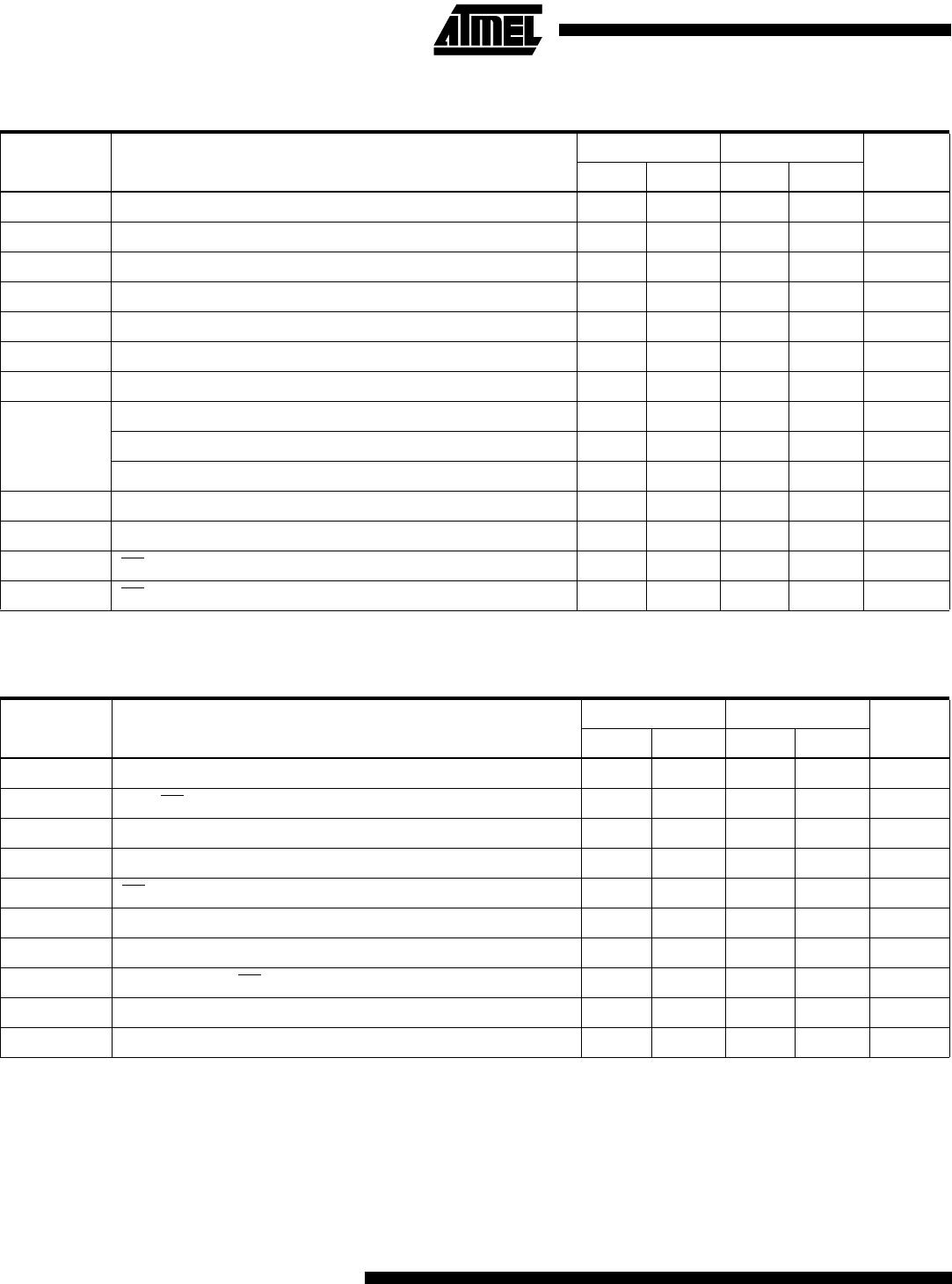
Input Test Waveforms and
Measurement Levels:
t
R
, t
F
< 1.5ns (10% to 90%)
Output Test Loads:
Commercial
Note: Similar devices are tested with slightly different loads.
These load differences may affect output signals’ delay
and slew rate. Atmel devices are tested with sufficient
margins to meet compatible devices.
Note: 1. Typical values for nominal supply voltage. This parameter is only sampled and is not 100% tested.
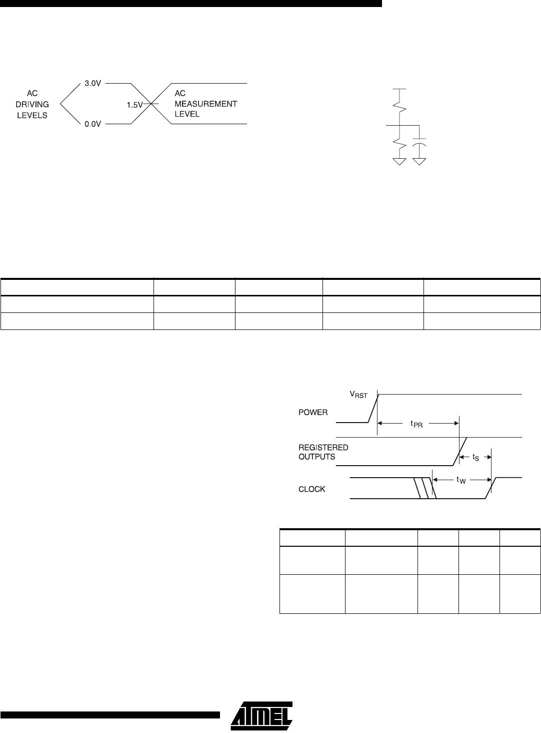
Power-up Reset
The ATF16LV8C’s registers are designed to reset during
power-up. At a point delayed slightly from V
CC
crossing
V
RST
, all registers will be reset to the low state. As a result,
the registered output state will always be high on power-up.
This feature is critical for state machine initialization.
However, due to the asynchronous nature of reset and the
uncertainty of how V
CC
actually rises in the system, the
following conditions are required:
1. The V
CC
rise must be monotonic from below 0.7V.
2. The signals from which the clock is derived must
remain stable during T
PR
.
3. After T
PR
, all input and feedback setup times must
be met before driving the clock term high.
OUTPUT
PIN
3.3V
CL = 35 pF
R1 = 316
R2 = 348
Pin Capacitance
(f = 1 MHz, T = 25°C)
(1)
Typ Max Units Conditions
C
IN
58 pF V
IN
= 0V
C
OUT
68 pF V
OUT
= 0V
Parameter Description Typ Max Units
T
PR
Power-up
Reset Time
600 1,000 ns
V
RST
Power-up
Reset
Voltage
2.5 3.0 V
ATF16LV8C
6
37.0
37.5
38.0
38.5
39.0
39.5
40.0
10 20 30 40 50 60 70 80 90 100
SUPPLY CURRENT
VS. INPUT FREQUENCY
(VCC = 3.3V, TA = 25°C)
ICC mA
FREQUENCY (MHz)
0
0.2
0.4
0.6
0.8
1.0
1.2
1.4
1.6
-5°
25°
75°
NORMALIZED SUPPLY CURRENT
VS. AMBIENT TEMPERATURE
(VCC = 3.3V, STANDBY)
AMBIENT TEMPERATURE (C)
NORM
ICC mA
20.5
21.0
21.5
22.0
22.5
23.0
23.5
24.0
24.5
25.0
3.0 3.15 3.3 3.45 3.6
OUTPUT SINK CURRENT
VS. SUPPLY VOLTAGE (TA = 25°C, VOL = 0.45V)
IOL mA
SUPPLY VOLTAGE (V)
0
10
20
30
40
50
60
0 0.1 0.2 0.3 0.4 0.5 0.6 0.7 0.8 0.9 1.0 1.1 1.2 1.3 1.4 1.5
IOL mA
OUTPUT VOLTAGE (V)
OUTPUT SINK CURRENT
VS. OUTPUT VOLTAGE (VCC = 5V, TA = 25°C)
3.0 3.3 3.6
1.6
1.4
1.2
1.0
0.8
0.6
0
NORMALIZED SUPPLY CURRENT
VS. SUPPLY VOLTAGE
(TA = 25°C, STANDBY)
SUPPLY VOLTAGE (V)
NORM
ICC mA
-16
-14
-12
-10
-8
-6
-4
-2
0
3.0
3.15 3.3
3.45
3.6
OUTPUT SOURCE CURRENT
VS. SUPPLY VOLTAGE (VOH = 2.4V, TA = 25°C)
IOH mA
SUPPLY VOLTAGE (V)

ATF16LV8C-10JU

Mfr. #:
Manufacturer:
Microchip Technology / Atmel
Description:
SPLD - Simple Programmable Logic Devices 250 GATE STANDARD POWER 3V - 10NS
Lifecycle:
New from this manufacturer.
Delivery:
DHL FedEx Ups TNT EMS
Payment:
T/T Paypal Visa MoneyGram Western Union