1. Product profile
1.1 General description
800 mA NPN low V
CEsat
Breakthrough In Small Signal (BISS) Resistor-Equipped
Transistors (RET) family in small plastic packages.
[1] Also available in SOT54A and SOT54 variant packages (see Section 2).
1.2 Features
1.3 Applications
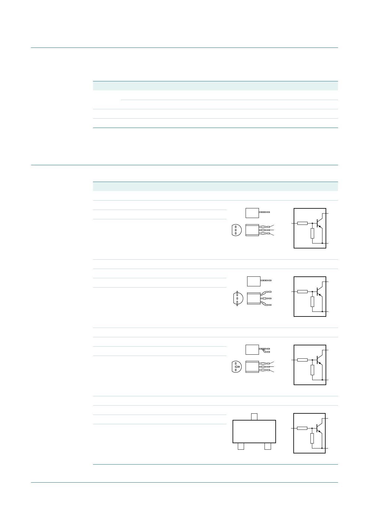
1.4 Quick reference data
PBRN113E series
NPN 800 mA, 40 V BISS RETs; R1 = 1 k, R2 = 1 k
Rev. 01 — 1 March 2007 Product data sheet
Table 1. Product overview
Type number Package
NXP JEITA JEDEC
PBRN113EK SOT346 SC-59A TO-236
PBRN113ES
[1]
SOT54 SC-43A TO-92
PBRN113ET SOT23 - TO-236AB
n 800 mA output current capability n Low collector-emitter saturation voltage
V
CEsat
n High current gain h
FE
n Reduces component count
n Built-in bias resistors n Reduces pick and place costs
n Simplifies circuit design n ±10 % resistor ratio tolerance
n Digital application in automotive and
industrial segments
n Switching loads
n Medium current peripheral driver
Table 2. Quick reference data
Symbol Parameter Conditions Min Typ Max Unit
V
CEO
collector-emitter voltage open base - - 40 V
I
O
output current
[1]
PBRN113EK, PBRN113ET - - 600 mA
PBRN113ES - - 800 mA
PBRN113E_SER_1 © NXP B.V. 2007. All rights reserved.
Product data sheet Rev. 01 — 1 March 2007 2 of 17
NXP Semiconductors
PBRN113E series
NPN 800 mA, 40 V BISS RETs; R1 = 1 k, R2 = 1 k
[1] Device mounted on an FR4 Printed-Circuit Board (PCB), single-sided copper, tin-plated and standard
footprint.
2. Pinning information
I
ORM
repetitive peak output current
PBRN113EK, PBRN113ET t
p
1 ms; δ≤0.33 - - 800 mA
R1 bias resistor 1 (input) 0.7 1 1.3 k
R2/R1 bias resistor ratio 0.9 1 1.1
Table 2. Quick reference data
…continued
Symbol Parameter Conditions Min Typ Max Unit
Table 3. Pinning
Pin Description Simplified outline Symbol
SOT54
1 input (base)
2 output (collector)
3 GND (emitter)
SOT54A
1 input (base)
2 output (collector)
3 GND (emitter)
SOT54 variant
1 input (base)
2 output (collector)
3 GND (emitter)
SOT23; SOT346
1 input (base)
2 GND (emitter)
3 output (collector)
001aab347
1
2
3
006aaa145
2
3
1
R1
R2
001aab348
1
2
3
006aaa145
2
3
1
R1
R2
001aab447
1
2
3
006aaa145
2
3
1
R1
R2
006aaa144
12
3
sym007
3
2
1
R1
R2
PBRN113E_SER_1 © NXP B.V. 2007. All rights reserved.
Product data sheet Rev. 01 — 1 March 2007 3 of 17
NXP Semiconductors
PBRN113E series
NPN 800 mA, 40 V BISS RETs; R1 = 1 k, R2 = 1 k
3. Ordering information
[1] Also available in SOT54A and SOT54 variant packages (see Section 2 and Section 9).
4. Marking
[1] * = -: made in Hong Kong
* = p: made in Hong Kong
* = t: made in Malaysia
* = W: made in China
5. Limiting values
Table 4. Ordering information
Type number Package
Name Description Version
PBRN113EK SC-59A plastic surface-mounted package; 3 leads SOT346
PBRN113ES
[1]
SC-43A plastic single-ended leaded (through hole) package;
3 leads
SOT54
PBRN113ET - plastic surface-mounted package; 3 leads SOT23
Table 5. Marking codes
Type number Marking code
[1]
PBRN113EK G1
PBRN113ES N113ES
PBRN113ET *7G
Table 6. Limiting values
In accordance with the Absolute Maximum Rating System (IEC 60134).
Symbol Parameter Conditions Min Max Unit
V
CBO
collector-base voltage open emitter - 40 V
V
CEO
collector-emitter voltage open base - 40 V
V
EBO
emitter-base voltage open collector - 10 V
V
I
input voltage
positive - +10 V
negative - 10 V
I
O
output current
PBRN113EK, PBRN113ET
[1]
- 600 mA
[2][3]
- 700 mA
PBRN113ES
[1]
- 800 mA
I
ORM
repetitive peak output current
PBRN113EK, PBRN113ET t
p
1 ms; δ≤0.33 - 800 mA

LTC6992IS6-1#TRPBF

Mfr. #:
Manufacturer:
Analog Devices Inc.
Description:
Switching Controllers PWM with 0% to 100% Pulse Width Control
Lifecycle:
New from this manufacturer.
Delivery:
DHL FedEx Ups TNT EMS
Payment:
T/T Paypal Visa MoneyGram Western Union