PBRN113E_SER_1 © NXP B.V. 2007. All rights reserved.
Product data sheet Rev. 01 — 1 March 2007 4 of 17
NXP Semiconductors
PBRN113E series
NPN 800 mA, 40 V BISS RETs; R1 = 1 kΩ, R2 = 1 kΩ
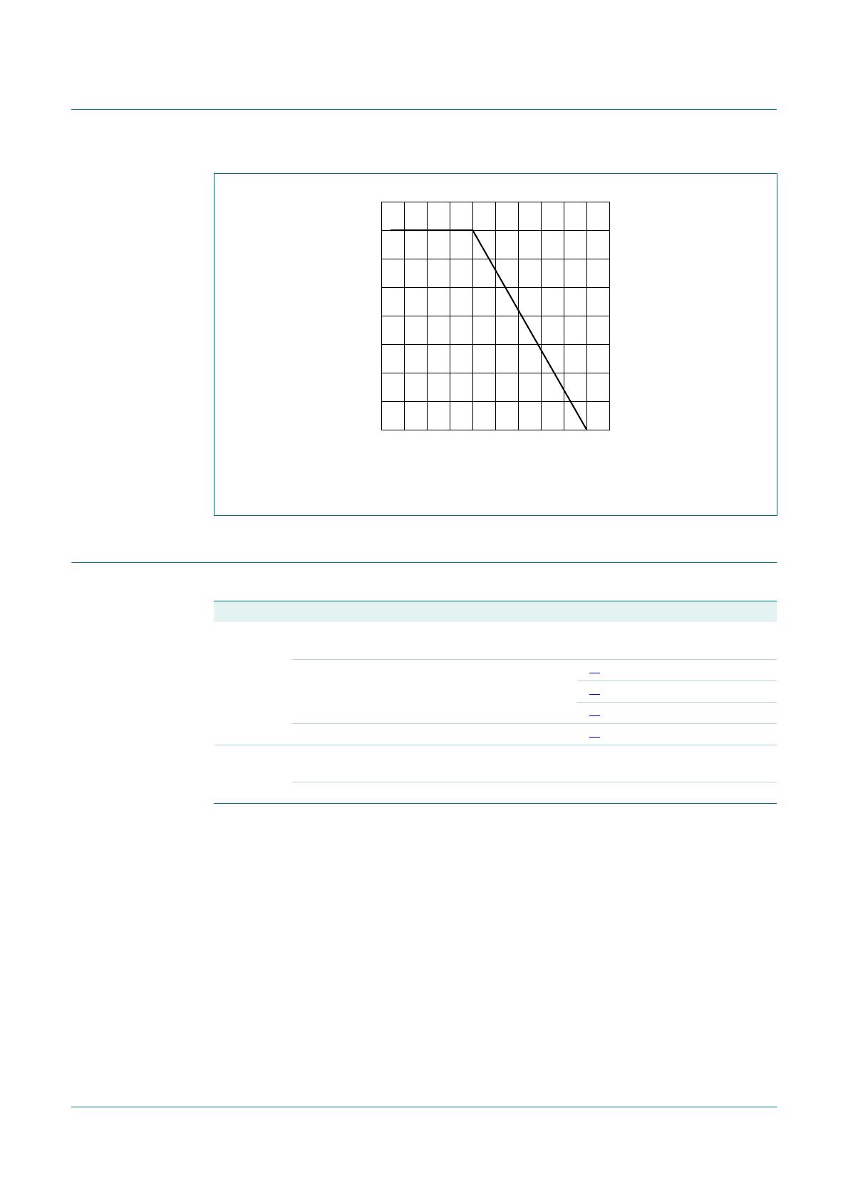
[1] Device mounted on an FR4 PCB, single-sided copper, tin-plated and standard footprint.
[2] Device mounted on an FR4 PCB, single-sided copper, tin-plated, mounting pad for collector 1 cm
2
.
[3] Device mounted on a ceramic PCB, Al
2
O
3
, standard footprint.
P
tot
total power dissipation T
amb
≤ 25 °C
PBRN113EK, PBRN113ET
[1]
- 250 mW
[2]
- 370 mW
[3]
- 570 mW
PBRN113ES
[1]
- 700 mW
T
j
junction temperature - 150 °C
T
amb
ambient temperature −65 +150 °C
T
stg
storage temperature −65 +150 °C
(1) Ceramic PCB, Al
2
O
3
, standard footprint
(2) FR4 PCB, mounting pad for collector 1 cm
2
(3) FR4 PCB, standard footprint
Fig 1. Power derating curves for SOT23 (TO-236AB) and SOT346 (SC-59A/TO-236)
Table 6. Limiting values
…continued
In accordance with the Absolute Maximum Rating System (IEC 60134).
Symbol Parameter Conditions Min Max Unit
T
amb
(°C)
−75 17512525 75−25
006aaa998
200
400
600
P
tot
(mW)
0
(1)
(2)
(3)