Data Sheet OP27
Rev. H | Page 15 of 21
COMMENTS ON NOISE
The OP27 is a very low noise, monolithic op amp. The out-
standing input voltage noise characteristics of the
OP27
are achieved mainly by operating the input stage at a high
quiescent current. The input bias and offset currents, which
would normally increase, are held to reasonable values by the
input bias current cancellation circuit. The OP27A/OP27E has
I
B
and I
OS
of only ±40 nA and 35 nA at 25°C respectively. This
is particularly important when the input has a high source
resistance. In addition, many audio amplifier designers prefer
to use direct coupling. The high I
B
, V
OS
, and TCV
OS
of previous
designs have made direct coupling difficult, if not impossible,
to use.
Voltage noise is inversely proportional to the square root of bias
current, but current noise is proportional to the square root of
bias current. The noise advantage of the
OP27 disappears when
high source resistors are used. Figure 38, Figure 39, Figure 40
compare the observed total noise of the
OP27 with the noise
performance of other devices in different circuit applications.
2/1
2
2
2
)(
)(
)
(
»
»
»
»
¼
º
«
«
«
«
¬
ª
u
NoiseResistor
RNoiseCurrent
NoiseVoltage
NoiseTotal
S
Figure 38 shows noise vs. source resistance at 1000 Hz. The
same plot applies to wideband noise. To use this plot, multiply
the vertical scale by the square root of the bandwidth.
R
S
—SOURCE RESISTANCE (
:
)
10
50 10k
5
500 1k 5k
1
100
50
100 50k
R
S1
R
S2
OP07
5534
OP27/37
REGISTER
NOISE ONLY
OP08/108
1
2
1 R
S
UNMATCHED
e.g. R
S
= R
S1
= 10k
:
, R
S2
= 0
2 R
S
MATCHED
e.g. R
S
= 10k
:
, R
S1
= R
S2
= 5k
:
00317-038
TOTAL NOIS
E (nV/
Hz)
Figure 38. Noise vs. Source Resistance (Including Resistor Noise) at 1000 Hz
At R
S
< 1 kΩ, the low voltage noise of the OP27 is maintained.
With R
S
< 1 kΩ, total noise increases but is dominated by the
resistor noise rather than current or voltage noise. lt is only
beyond R
S
of 20 kΩ that current noise starts to dominate. The
argument can be made that current noise is not important for
applications with low-to-moderate source resistances. The
crossover between the
OP27 and OP07 noise occurs in the 15 k
to 40 kΩ region.
Figure 39 shows the 0.1 Hz to 10 Hz p-p noise. Here the picture
is less favorable; resistor noise is negligible and current noise
becomes important because it is inversely proportional to the
square root of frequency. The crossover with the
OP07 occurs
in the 3 kΩ to 5 kΩ range depending on whether balanced or
unbalanced source resistors are used (at 3 kΩ the I
B
and I
OS
error also can be 3× the V
OS
spec).
R
S
—SOURCE RESISTANCE (
:
)
100
50
10k
p-p NOISE (nV)
50
500 1k
5k
10
1k
500
100 50k
R
S1
R
S2
1 R
S
UNMATCHED
e.g. R
S
= R
S1
= 10k
:
, R
S2
= 0
2 R
S
MATCHED
e.g. R
S
= 10k
:
, R
S1
= R
S2
= 5k
:
OP07
5534
OP27/37
REGISTER
NOISE ONLY
OP08/108
1
2
00317-039
Figure 39. Peak-to-Peak Noise (0.1 Hz to 10 Hz) as Source Resistance
(Includes Resistor Noise)
For low frequency applications, the OP07 is better than the
OP27/OP37 when RS > 3 kΩ. The only exception is when gain
error is important.
Figure 40 illustrates the 10 Hz noise. As expected, the results are
between the previous two figures.
10
50
10k
5
500 1k 5k
1
100
50
100 50k
OP07
5534
OP27/37
REGISTER
NOISE ONLY
OP08/108
R
S1
R
S2
1 R
S
UNMATCHED
e.g. R
S
= R
S1
= 10k
:
, R
S2
= 0
2 R
S
MA
TCHED
e.g. R
S
= 10k
:
, R
S1
= R
S2
= 5k
:
1
2
00317-040
R
S
—SOURCE RESISTANCE (
:
)
TOTAL NOISE (nV/
Hz)
Figure 40. 10 Hz Noise vs. Source Resistance (Includes Resistor Noise)
Audio Applications
OP27 Data Sheet
Rev. H | Page 16 of 21
For reference, typical source resistances of some signal sources
are listed in Table 7.
Table 7.
Device
Source
Impedance Comments
Strain Gauge <500 Ω Typically used in low frequency
applications.
Magnetic
Tape Head
<1500 Ω Low is very important to reduce
self-magnetization problems
when direct coupling is used.
OP27 IB can be neglected.
Magnetic
Phonograph
Cartridges
<1500 Ω
Similar need for low I
B
in direct
coupled applications. OP27 does
not introduce any self-
magnetization problems.
Linear
Variable
Differential
Transformer
<1500 Ω Used in rugged servo-feedback
applications. Bandwidth of
interest is 400 Hz to 5 kHz.
Table 8. Open-Loop Gain
Frequency OP07 OP27 OP37
At 3 Hz 100 dB 124 dB 125 dB
At 10 Hz 100 dB 120 dB 125 dB
At 30 Hz 90 dB 110 dB 124 dB
AUDIO APPLICATIONS
Figure 41 is an example of a phono pre-amplifier circuit using the
OP27 for A1; R1-R2-C1-C2 form a very accurate RIAA network
with standard component values. The popular method to
accomplish RIAA phono equalization is to employ frequency
dependent feedback around a high quality gain block. Properly
chosen, an RC network can provide the three necessary time
constants of 3180 µs, 318 µs, and 75 µs.
For initial equalization accuracy and stability, precision metal
film resistors and film capacitors of polystyrene or polypro-
pylene are recommended because they have low voltage
coefficients, dissipation factors, and dielectric absorption.
(High-k ceramic capacitors should be avoided here, though
low-k ceramics, such as NPO types that have excellent
dissipation factors and somewhat lower dielectric absorption,
can be considered for small values.)
C
A
150pF
A1
OP27
R
A
N
MOVING MAGNET
CARTRIDGE INPUT
+ +
C4 (2)
220µF
C1
0.03µF
C2
0.01µF
C3
0.47µF
LF ROLLOFF
OUT IN
OUTPUT
R5
N
R4
N
R1
N
R2
N
R3

G = 1kHz GAIN
= 0.101 ( 1 + )
R1
R3
= 98.677 (39.9dB)
AS SHOWN
2
6
3
00317-041
Figure 41. Phono Preamplifier Circuit
The OP27 brings a 3.2 nV/√Hz voltage noise and 0.45 pA/Hz
current noise to this circuit. To minimize noise from other
sources, R3 is set to a value of 100 Ω, generating a voltage noise
of 1.3 nV/√Hz. The noise increases the 3.2 nV/√Hz of the
amplifier by only 0.7 dB. With a 1 kΩ source, the circuit noise
measures 63 dB below a 1 mV reference level, unweighted, in a
20 kHz noise bandwidth.
Gain (G) of the circuit at 1 kHz can be calculated by the
expression:
¸
¹
·
¨
©
§
R3
R1
G 1101.0
For the values shown, the gain is just under 100 (or 40 dB).
Lower gains can be accommodated by increasing R3, but gains
higher than 40 dB show more equalization errors because of the
8 MHz gain bandwidth of the
OP27.
This circuit is capable of very low distortion over its entire
range, generally below 0.01% at levels up to 7 V rms. At 3 V
output levels, it produces less than 0.03% total harmonic
distortion at frequencies up to 20 kHz.
Capacitor C3 and Resistor R4 form a simple −6 dB per octave
rumble filter, with a corner at 22 Hz. As an option, the switch
selected Shunt Capacitor C4, a nonpolarized electrolytic,
bypasses the low frequency roll-off. Placing the rumble filter’s
high-pass action after the preamplifier has the desirable result
of discriminating against the RIAA-amplified low frequency
noise components and pickup produced low frequency
disturbances.
A preamplifier for NAB tape playback is similar to an RIAA
phono preamplifier, though more gain is typically demanded,
along with equalization requiring a heavy low frequency boost.
The circuit in Figure 41 can be readily modified for tape use, as
shown by Figure 42.
Data Sheet OP27
Rev. H | Page 17 of 21
C
A
R
A
R1
N
R2
N
TAPE
HEAD
0.47µF
0.01µF

N
T1 = 3180µs
T2 = 50µs
OP27
+
00317-042
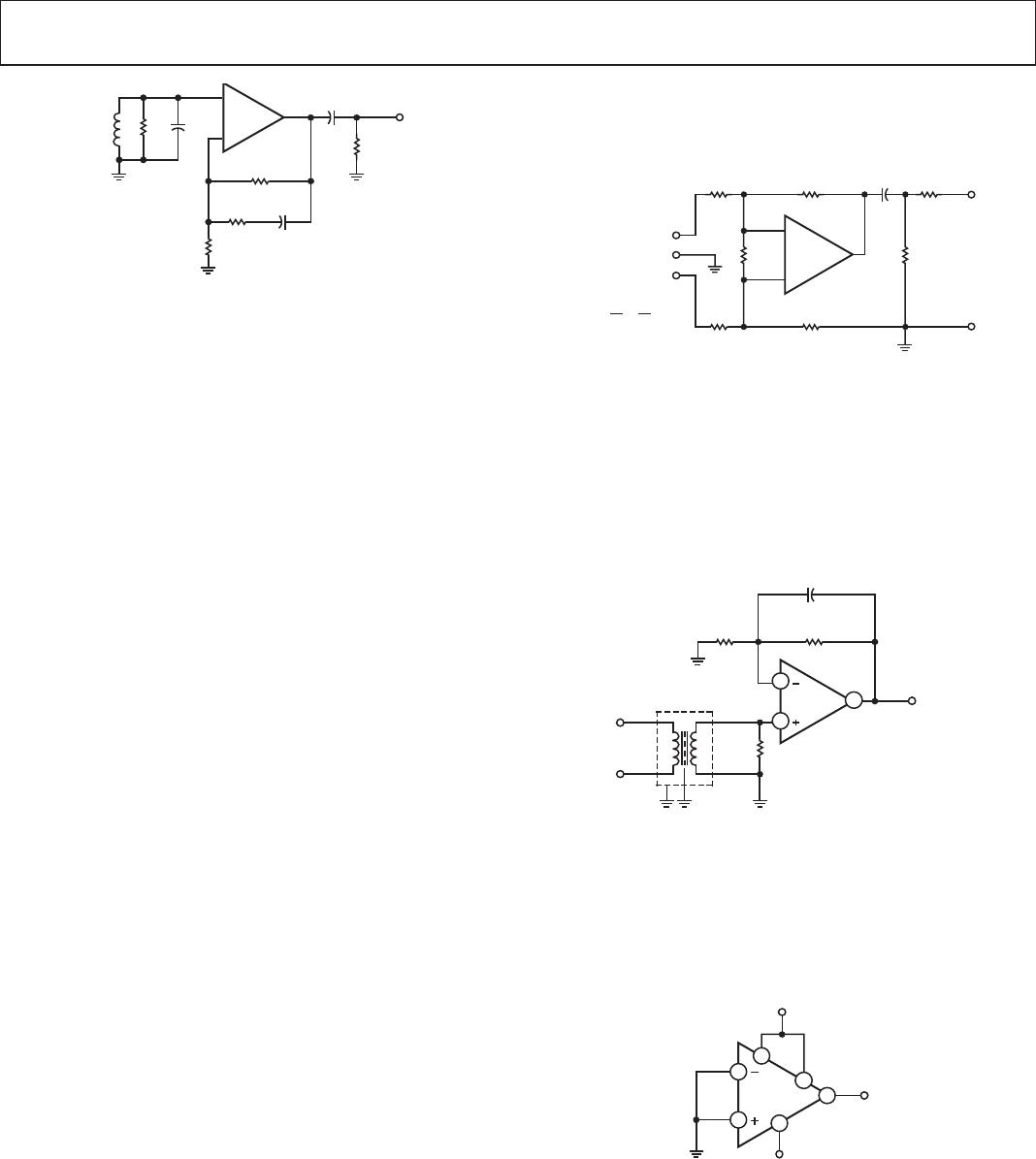
Figure 42. Tape Head Preamplifier
While the tape equalization requirement has a flat high
frequency gain above 3 kHz (T2 = 50 µs), the amplifier need
not be stabilized for unity gain. The decompensated
OP37
provides a greater bandwidth and slew rate. For many applica-
tions, the idealized time constants shown can require trimming
of R1 and R2 to optimize frequency response for nonideal tape
head performance and other factors (see the References section).
The network values of the configuration yield a 50 dB gain at
1 kHz, and the dc gain is greater than 70 dB. Thus, the worst-
case output offset is just over 500 mV. A single 0.47 µF output
capacitor can block this level without affecting the dynamic
range.
The tape head can be coupled directly to the amplifier input,
because the worst-case bias current of 80 nA with a 400 mH,
100 µ inch head (such as the PRB2H7K) is not troublesome.
Amplifier bias-current transients that can magnetize a head
present one potential tape head problem. The
OP27 and OP37
are free of bias current transients upon power-up or power-
down. It is always advantageous to control the speed of power
supply rise and fall to eliminate transients.
In addition, the dc resistance of the head should be carefully
controlled and preferably below 1 kΩ. For this configuration,
the bias current induced offset voltage can be greater than the
100 pV maximum offset if the head resistance is not sufficiently
controlled.
A simple, but effective, fixed gain transformerless microphone
preamp (Figure 43) amplifies differential signals from low
impedance microphones by 50 dB and has an input impedance
of 2 kΩ. Because of the high working gain of the circuit, an
OP37 helps to preserve bandwidth, which is 110 kHz. As the
OP37 is a decompensated device (minimum stable gain of 5), a
dummy resistor, R
p
, may be necessary if the microphone is to be
unplugged. Otherwise, the 100% feedback from the open input
can cause the amplifier to oscillate.
Common-mode input noise rejection will depend upon the
match of the bridge-resistor ratios. Either close tolerance (0.1%)
types should be used, or R4 should be trimmed for best CMRR.
All resistors should be metal film types for best stability and low
noise.
Noise performance of this circuit is limited more by the Input
Resistors R1 and R2 than by the op amp, as R1 and R2 each
generate a 4 nV/√Hz noise, while the op amp generates a
3.2 nV/√Hz noise. The rms sum of these predominant noise
sources is about 6 nV/√Hz, equivalent to 0.9 µV in a 20 kHz
noise bandwidth, or nearly 61 dB below a 1 mV input signal.
Measurements confirm this predicted performance.
LOW IMPEDANCE
MICROPHONE INPUT
=  T2
C1
5mF
R1
N
R3
N
R6

R4
N
R2
N
R
P
N
OUTPUT
R3
R1
R4
R2
=
OP27/
OP37
+
R7
N
00317-043
Figure 43. Fixed Gain Transformerless Microphone Preamplifier
For applications demanding appreciably lower noise, a high
quality microphone transformer coupled preamplifier (Figure 44)
incorporates the internally compensated
OP27. T1 is a JE-
115K-E 150 Ω/15 kΩ transformer that provides an optimum
source resistance for the
OP27 device. The circuit has an overall
gain of 40 dB, the product of the transformer’s voltage setup and
the op amps voltage gain.
JENSEN TRANSFORMERS
A1
OP27
R3

R1

R2
1
C2
1800pF
OUTPUT

SOURCE
T1
1
T1 – JENSEN JE – 115K – E
1
3
6
2
00317-044
Figure 44. High Quality Microphone Transformer Coupled Preamplifier
Gain can be trimmed to other levels, if desired, by adjusting R2
or R1. Because of the low offset voltage of the
OP27, the output
offset of this circuit is very low, 1.7 mV or less, for a 40 dB gain.
The typical output blocking capacitor can be eliminated in such
cases, but it is desirable for higher gains to eliminate switching
transients.
OP27
–18V
+18V
8
7
6
4
3
2
00317-045
Figure 45. Burn-In Circuit
Capacitor C2 and Resistor R2 form a 2 µs time constant in this
circuit, as recommended for optimum transient response by the
transformer manufacturer. With C2 in use, A1 must have unity-
gain stability. For situations where the 2 µs time constant is not
necessary, C2 can be deleted, allowing the faster
OP37 to be
employed.

OP27GSZ

Mfr. #:
Manufacturer:
Analog Devices Inc.
Description:
Precision Amplifiers LOW-NOISE PREC IC 2.8V/uS
Lifecycle:
New from this manufacturer.
Delivery:
DHL FedEx Ups TNT EMS
Payment:
T/T Paypal Visa MoneyGram Western Union