2
COMMERCIAL TEMPERATURE RANGE
IDT7280/7281/7282/7283/7284/7285 5V ASYNCHRONOUS FIFO
DUAL 256 x 9, 512 x 9, 1,024 x 9, 2,048 x 9, 4,096 x 9 and 8,192 x 9
JUNE 29, 2012
PIN CONFIGURATION ABSOLUTE MAXIMUM RATINGS
Symbol Rating Com'l & Ind'l Unit
V
TERM Terminal Voltage with –0.5 to +7.0 V
Respect to GND
TSTG Storage Temperature –55 to +125 °C
I
OUT DC Output Current –50 to +50 mA
NOTE:
1. Stresses greater than those listed under ABSOLUTE MAXIMUM RATINGS may cause
permanent damage to the device. This is a stress rating only and functional operation
of the device at these or any other conditions above those indicated in the operational
sections of this specification is not implied. Exposure to absolute maximum rating
conditions for extended periods may affect reliability.
AC TEST CONDITIONS
Input Pulse Levels GND to 3.0V
Input Rise/Fall Times 5ns
Input Timing Reference Levels 1.5V
Output Reference Levels 1.5V
Output Load See Figure 1
CAPACITANCE (TA = +25
o
C, f = 1.0 MHz)
Symbol Parameter Condition Max. Unit
CIN Input Capacitance VIN = 0V 8 pF
C
OUT Output Capacitance VOUT = 0V 8 pF
NOTE:
1. Characterized values, not currently tested.
Symbol Parameter Min. Typ. Max. Unit
VCC Supply Voltage 4.5 5.0 5.5 V
GND Supply Voltage 0 0 0 V
VIH
(1)
Input High Voltage 2.0 — — V
VIL
(2)
Input Low Voltage — — 0.8 V
TA Operating Temperature 0 — 70 °C
Commercial
TA Operating Temperature –40 — 85 °C
Industrial
NOTES:
1. For RT/RS/XI input, VIH = 2.6V (commercial).
2. 1.5V undershoots are allowed for 10ns once per cycle.
RECOMMENDED DC OPERATING
CONDITIONS
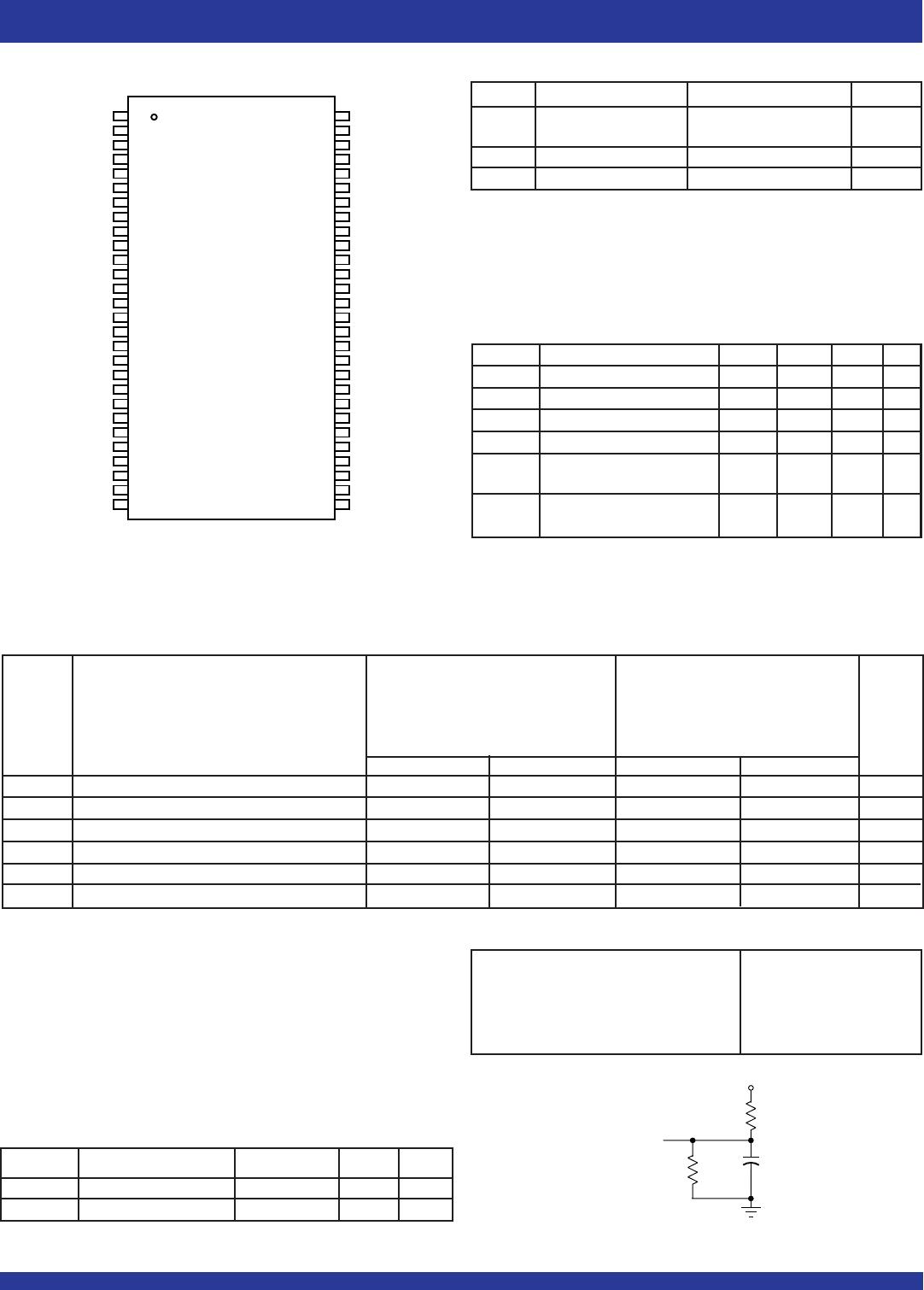
TSSOP (SO56-2, order code: PA)
TOP VIEW
FFA
QA
0
QA1
QA2
QA3
QA8
GND
RA
QA
4
QA5
QA6
QA7
XOA/HFA
EFA
FFB
QB
0
QB1
QB2
QB3
QB8
GND
RB
QB
4
QB5
QB6
QB7
XOB/HFB
EFB
1
2
3
4
5
6
7
8
9
10
11
12
13
14
15
16
17
18
19
20
21
22
23
24
25
26
27
28
XIA
DA
0
DA1
DA2
DA3
DA8
WA
V
CC
DA4
DA5
DA6
DA7
FLA/RTA
RSA
XIB
DB
0
DB1
DB2
DB3
DB8
WB
V
CC
DB4
DB5
DB6
DB7
FLB/RTB
RSB
56
55
54
53
52
51
50
49
48
47
46
45
44
43
42
41
40
39
38
37
36
35
34
33
32
31
30
29
3208 drw 02
3208 drw 03
30pF*
1.1K
5V
TO
OUTPUT
PIN
680Ω
or equivalent circuit
IDT7280L IDT7283L
IDT7281L IDT7284L
IDT7282L IDT7285lL
Commercial & Industrial
(1)
Commercial & Industrial
(1)
tA = 12, 15 ns tA = 12, 15 ns
Symbol Parameter Min. Max. Min. Max. Unit
I
LI
(2)
Input Leakage Current (Any Input) –1 1 –1 — μA
ILO
(3)
Output Leakage Current –10 10 –10 10 μA
V
OH Output Logic “1” Voltage IOH = –2mA 2.4 — 2.4 — V
VOL Output Logic “0” Voltage IOL = 8mA — 0.4 — 0.4 V
ICC1
(4,5)
Active Power Supply Current (both FIFOs) — 125
(6)
—150mA
I
CC2
(4,7)
Standby Current (R=W=RS=FL/RT=VIH)—15—15mA
DC ELECTRICAL CHARACTERISTICS
(Commercial: VCC = 5V ± 10%, TA = 0°C to +70°C; Industrial: VCC = 5V ± 10%, TA = –40°C to +85°C)
NOTES:
1.
Industrial temperature range product for the 15ns speed grade is available as a standard
device.
2. Measurements with 0.4 ≤ VIN ≤ VCC.
3. R ≥ VIH, 0.4 ≤ VOUT ≤ VCC.
4. Tested with outputs open (IOUT = 0).
5. Tested at f = 20 MHz.
6. Typical ICC1 = 2*[15 + 2*fS + 0.02*CL*fS] (in mA) with VCC = 5V, TA = 25
o
C, fS = WCLK
frequency = RCLK frequency (in MHz, using TTL levels), data switching at fS/2,
CL = capacitive load (in pF).
7. All Inputs = VCC - 0.2V or GND + 0.2V.
Figure 1. Output Load
* Includes scope and jig capacitances.