ISL55015IEZ-T7

1
DATASHEET
MMIC Silicon Bipolar Broadband Amplifier
ISL55015
The ISL55015 is a high performance gain block featuring a
Darlington configuration using high f
T
transistors and excellent
thermal performance. They are an ideal choice for DVB-S LNB
cable receiver applications.
Other members of the family include:
ISL55012 and ISL55015 match a 75Ω source to a 50Ω load
ISL55014 matches a 50Ω source to a 50Ω load
Related Literature
For a full list of related documents, visit our website
- ISL55015 product page
Features
Input impedance of 75Ω
Output impedance of 50Ω
Gain of 13.5dB at 1GHz
Noise figure of 4.8dB at 2GHz
OIP3 of 31dBm at 1GHz
Low input and output return losses
Pb-free (RoHS compliant)
Applications
LNB and LNB-T (HDTV) amplifiers
IF gain blocks for satellite and terrestrial STBs
PA driver amplifier
Wireless data, satellite
Bluetooth/WiFi
Satellite locator and signal strength meters
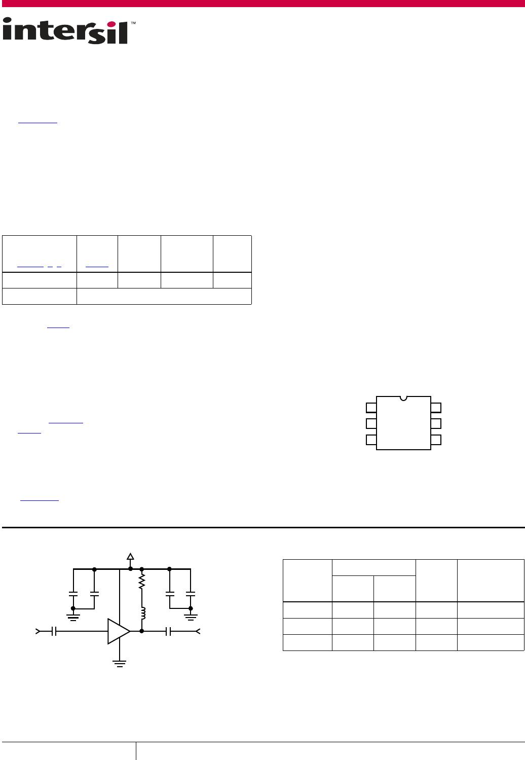
Pin Configuration
ISL55015
(6 LD SC-70)
TOP VIEW
Ordering Information
PART
NUMBER
(Notes 1
, 2, 3)
PART
MARKING
(Note 4
)
TAPE AND
REEL
(UNITS)
PACKAGE
(RoHS
COMPLIANT)
PKG.
DWG. #
ISL55015IEZ-T7 CCK 3k 6 Ld SC-70 P6.049B
ISL55015IEZ-EVAL Evaluation board
NOTES:
1. Refer to TB347
for details on reel specifications.
2. These Intersil Pb-free plastic packaged products employ special
Pb-free material sets, molding compounds/die attach materials,
and 100% matte tin plate plus anneal (e3 termination finish, which
is RoHS compliant and compatible with both SnPb and Pb-free
soldering operations). Intersil Pb-free products are MSL classified at
Pb-free peak reflow temperatures that meet or exceed the Pb-free
requirements of IPC/JEDEC J STD-020.
3. For Moisture Sensitivity Level (MSL), please see device information
page for ISL55015
. For more information on MSL please techbrief
TB363
.
4. The part marking is located on the bottom of the part.
GND
GND
IN
1
2
3
6
5
4
OUT
GND
VSP
FIGURE 1. TYPICAL APPLICATION CIRCUIT
100pF
0.1µF
100nH
100pF
0.1µF
68pF
68pF
1, 2, 5
3
4
6
+5V
24Ω
TABLE 1. KEY DIFFERENCES BETWEEN FAMILY OF PARTS
PART #
IMPEDANCE
GAIN
AT 1GHz
(dB)
NOISE FIGURE
AT 2GHz
(dB)
SOURCE
(Ω)
LOAD
(Ω)
ISL55012 75 50 18 4.7
ISL55014 50 50 17.2 4.3
ISL55015 75 50 13.5 4.8
February 6, 2017
FN6284.3
CAUTION: These devices are sensitive to electrostatic discharge; follow proper IC Handling Procedures.
1-888-INTERSIL or 1-888-468-3774
| Copyright Intersil Americas LLC 2006, 2007, 2013, 2017. All Rights Reserved
Intersil (and design) is a trademark owned by Intersil Corporation or one of its subsidiaries.
All other trademarks mentioned are the property of their respective owners.
ISL55015
2
FN6284.3
February 6, 2017
Submit Document Feedback
Absolute Maximum Ratings (T
A
= +25°C) Thermal Information
Supply Voltage from V
SP
to GND . . . . . . . . . . . . . . . . . . . . . . . . . . . . . . . . 6V
Input Voltage. . . . . . . . . . . . . . . . . . . . . . . . . . . . . . V
S
+ +0.3V to GND - 0.3V
ESD Rating
Human Body Model (Per MIL-STD-883 Method 3015.7). . . . . . . . 6000V
Machine Model (Per EIAJ ED-4701 Method C-111) . . . . . . . . . . . . . 250V
Thermal Resistance (Typical)
JA
(°C/W)
JC
(°C/W)
6 Ld SC-70 (Notes 5
, 6) . . . . . . . . . . . . . . . . 255 195
Storage Temperature . . . . . . . . . . . . . . . . . . . . . . . . . . . . . .-65°C to +125°C
Operating Junction Temperature . . . . . . . . . . . . . . . . . . . . . . . . . . . .+135°C
Pb-Free Reflow Profile . . . . . . . . . . . . . . . . . . . . . . . . . . . . . . . . . . see TB493
Recommended Operating Conditions
Ambient Operating Temperature . . . . . . . . . . . . . . . . . . . . .-40°C to +85°C
CAUTION: Do not operate at or near the maximum ratings listed for extended periods of time. Exposure to such conditions may adversely impact product
reliability and result in failures not covered by warranty.
NOTES:
5.
JA
is measured with the component mounted on a high-effective thermal conductivity test board in free air. See Tech Brief TB379 for details.
6. For
JC
, the “case temp” location is taken at the package top center.
Electrical Specifications V
SP
= +5V, Z
RSC
= Z
LOAD
= 50Ω, T
A
= +25°C, 24Ω V
SP
to OUT, unless otherwise specified.
PARAMETER SYMBOL TEST CONDITIONS
MIN
(Note 7
)TYP
MAX
(Note 7)UNIT
Supply Voltage V
SP
To operate below 5V, the 24Ω resistor to supply
should be reduced
3.0 5.5 V
Small Signal Gain Gt 1.0GHz 12.3 13.5 14.8 dB
1.5GHz 11.7 13.3 14.2 dB
2.0GHz 11.0 12.4 13.5 dB
Output Power at 1dB Compression P1dB 1.0GHz 16.4 18.1 21.6 dBm
2.0GHz 15.3 19.4 21.0 dBm
Output Third Order Intercept Point OIP3 1.0GHz 31.3 dBm
2.0GHz 28.4 dBm
Output Second Order Intercept Point OIP2 Input tones at 1.0GHz and 1.1GHz, at Input
Power = -15dBm, Output tone 2.1GHz
47 dBm
3dB Bandwidth BW 3dB below Gain at 500MHz 2.9 GHz
Input Return Loss IRL 1.0GHz Z
RSC
= 75Ω, Z
LOAD
= 50Ω 20.2 dB
Output Return Loss ORL 1.0GHz Z
RSC
= 75Ω, Z
LOAD
= 50Ω 21.4 dB
Reverse Isolation RISOL 2.0GHz 18.9 dB
Noise Figure NF 2.0GHz 4.8 dB
Device Operating Current ID 54 62.5 69 mA
NOTE:
7. Parameters with MIN and/or MAX limits are 100% tested at +25°C, unless otherwise specified. Temperature limits established by characterization
and are not production tested.
ISL55015
3
FN6284.3
February 6, 2017
Submit Document Feedback
Device Test Setup
50Ω50Ω
50Ω 50Ω
5V
VNA
DC BLOCK DUT BIAS TEE
5V
POWER
SUPPLY
PICOSECOND LABS
MODEL 5508-110
PICOSECOND LABS
MODEL 5542
CONNECTORLESS
PLATFORM
AGILENT _8753ES
INPUT
REFERENCE
PLANE
OUTPUT
REFERENCE
PLANE
I
DEVICE
PIN 3 PIN 6
I
1
I
2
24Ω
FIGURE 2. DEVICE TEST SETUP
Typical Performance Curves Z
SRC
= 75Ω, Z
LOAD
= 50Ω
FIGURE 3. INPUT RETURN LOSS vs FREQUENCY FIGURE 4. OUTPUT RETURN LOSS vs FREQUENCY
0
5
10
15
20
25
0.5 1.0 1.5 2.0 2.5 3.0
FREQUENCY (GHz)
IRL (dB)
0
5
10
15
20
25
0.5 1.0 1.5 2.0 2.5 3.0
FREQUENCY (GHz)
ORL (dB)
Typical Performance Curves 50Ω environment
FIGURE 5. |S21| vs FREQUENCY FIGURE 6. |S11| vs FREQUENCY
10
12
14
16
0.5
1.0 1.5 2.0 2.5 3.0
FREQUENCY (GHz)
S21 (dB)
-14
-12
-10
-8
-6
-4
-2
0
0.5 1.0 1.5 2.0 2.5 3.0
FREQUENCY (GHz)
S11 (dB)

ISL55015IEZ-T7

Mfr. #:
Manufacturer:
Renesas / Intersil
Description:
RF Amplifier ISL59444IBZ 1GHZ 4X1 VID CROSPOINT SWITCH
Lifecycle:
New from this manufacturer.
Delivery:
DHL FedEx Ups TNT EMS
Payment:
T/T Paypal Visa MoneyGram Western Union

Products related to this Datasheet