VS-VSK.170PbF, VS-VSK.250PbF Series
www.vishay.com
Vishay Semiconductors
Revision: 09-Feb-17
3
Document Number: 94417
For technical questions within your region: DiodesAmericas@vishay.com
, DiodesAsia@vishay.com, DiodesEurope@vishay.com
THIS DOCUMENT IS SUBJECT TO CHANGE WITHOUT NOTICE. THE PRODUCTS DESCRIBED HEREIN AND THIS DOCUMENT
ARE SUBJECT TO SPECIFIC DISCLAIMERS, SET FORTH AT www.vishay.com/doc?91000
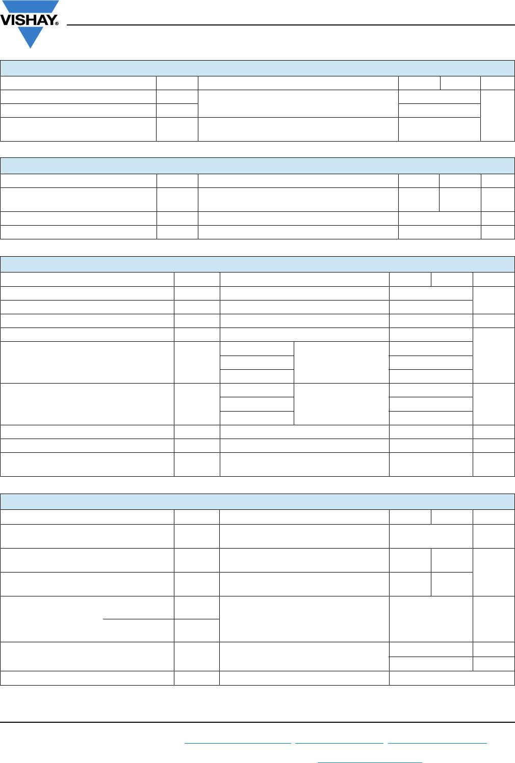
SWITCHING
PARAMETER SYMBOL TEST CONDITIONS VSK.170 VSK.250 UNITS
Typical delay time t
d
T
J
= 25 °C, gate current = 1 A dI
g
/dt = 1 A/μs
V
d
= 0.67 % V
DRM
1.0
μs
Typical rise time t
r
2.0
Typical turn-off time t
q
I
TM
= 300 A; dI/dt = 15 A/μs; T
J
= T
J
maximum;
V
R
= 50 V; dV/dt = 20 V/μs; gate 0 V, 100
50 to 150
BLOCKING
PARAMETER SYMBOL TEST CONDITIONS VSK.170 VSK.250 UNITS
Maximum peak reverse and
off-state leakage current
I
RRM,
I
DRM
T
J
= T
J
maximum 50 60 mA
RMS insulation voltage V
INS
50 Hz, circuit to base, all terminals shorted, 25 °C, 1 s 3000 V
Critical rate of rise of off-state voltage dV/dt T
J
= T
J
maximum, exponential to 67 % rated V
DRM
1000 V/μs
TRIGGERING
PARAMETER SYMBOL TEST CONDITIONS VSK.170 VSK.250 UNITS
Maximum peak gate power P
GM
t
p
5 ms, T
J
= T
J
maximum 10.0
W
Maximum average gate power P
G(AV)
f = 50 Hz, T
J
= T
J
maximum 2.0
Maximum peak gate current + I
GM
t
p
5 ms, T
J
= T
J
maximum 3.0 A
Maximum peak negative gate voltage - V
GT
t
p
5 ms, T
J
= T
J
maximum 5.0
V
Maximum required DC gate voltage to trigger V
GT
T
J
= - 40 °C
Anode supply = 12 V,
resistive load; Ra = 1
4.0
T
J
= 25 °C 3.0
T
J
= T
J
maximum 2.0
Maximum required DC gate current to trigger I
GT
T
J
= - 40 °C
Anode supply = 12 V,
resistive load; Ra = 1
350
mAT
J
= 25 °C 200
T
J
= T
J
maximum 100
Maximum gate voltage that will not trigger V
GD
T
J
= T
J
maximum, rated V
DRM
applied 0.25 V
Maximum gate current that willnot trigger I
GD
T
J
= T
J
maximum, rated V
DRM
applied 10.0 mA
Maximum rate of rise of turned-on current dI/dt
T
J
= T
J
maximum, I
TM
= 400 A,
rated V
DRM
applied
500 A/μs
THERMAL AND MECHANICAL SPECIFICATIONS
PARAMETER SYMBOL TEST CONDITIONS VSK.170 VSK.250 UNITS
Junction operating and storage
temperature range
T
J
, T
Stg
-40 to +130 °C
Maximum thermal resistance,
junction to case per junction
R
thJC
DC operation 0.17 0.125
K/W
Typical thermal resistance,
case to heatsink per module
R
thCS
Mounting surface flat, smooth and greased 0.02 0.02
Mounting torque ± 10 %
MAP to heatsink
A mounting compound is recommended
and the torque should be rechecked after
a period of about 3 hours to allow for the
spread of the compound.
4 to 6 Nm
busbar to MAP
Approximate weight
500 g
17.8 oz.
Case style MAGN-A-PAK

