VS-VSK.170PbF, VS-VSK.250PbF Series
www.vishay.com
Vishay Semiconductors
Revision: 09-Feb-17
7
Document Number: 94417
For technical questions within your region: DiodesAmericas@vishay.com
, DiodesAsia@vishay.com, DiodesEurope@vishay.com
THIS DOCUMENT IS SUBJECT TO CHANGE WITHOUT NOTICE. THE PRODUCTS DESCRIBED HEREIN AND THIS DOCUMENT
ARE SUBJECT TO SPECIFIC DISCLAIMERS, SET FORTH AT www.vishay.com/doc?91000
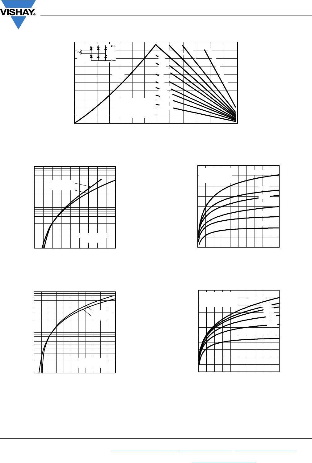
Fig. 14 - Maximum Non-Repetitive Surge Current Fig. 15 - Maximum Non-Repetitive Surge Current
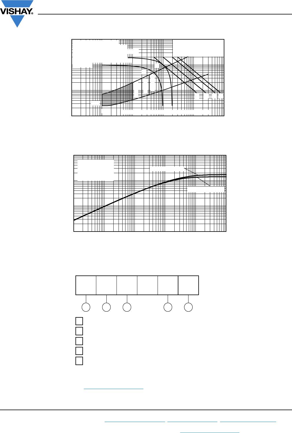
Fig. 16 - On-State Power Loss Characteristics
Fig. 17 - On-State Power Loss Characteristics
3500
4000
4500
5000
5500
6000
6500
7000
7500
11010
0
Number Of Equal Amplitude Half Cycle Current Pulses (N)
Peak Half Sine Wave On-state Current (A)
VSK.250.. series
per junction
At any rated load condition and with
rated V
RRM
applied following surge.
Initial T = 130 °C
at 60 Hz 0.0083 s
at 50 Hz 0.0100 s
J
3000
4000
5000
6000
7000
8000
9000
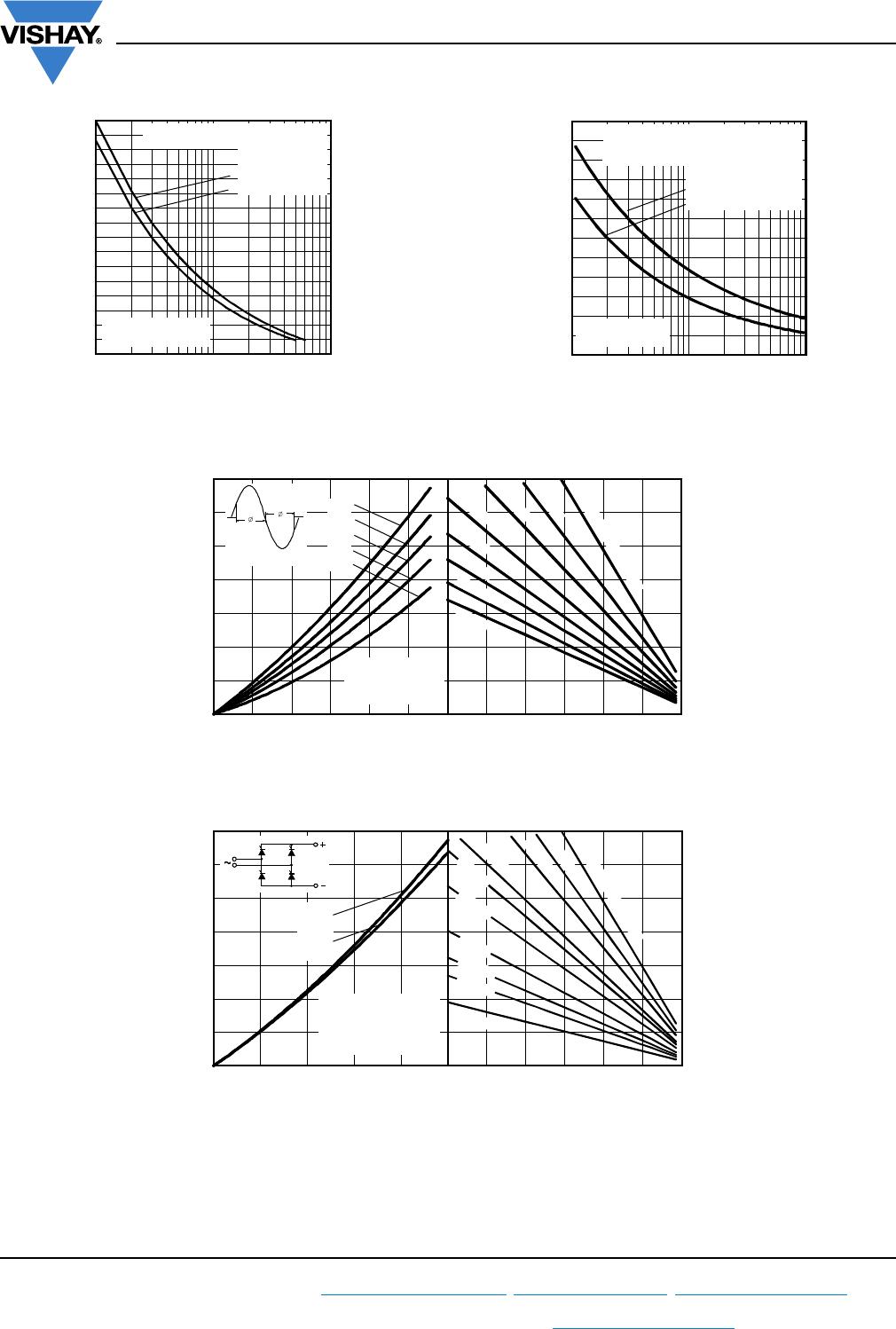
0.01 0.1 1
Peak Half Sine Wave On-state Current (A)
Pulse Train Duration (s)
Maximum non-repetitive surge Current
vs. pulse train duration. Control of
conduction may not be maintained.
VSK.250.. series
per junction
Initial T
J
= 130 °C
No voltage reapplied
Rated V
RRM
reapplied
020406080100120
Maximum Allowable Ambient Temperature (°C)
0
.
3
K
/
W
0
.
2
5
K
/
W
0
.
2
0
K
/
W
0
.
1
6
K
/
W
0
.
1
2
K
/
W
0
.
0
8
K
/
W
0
.
0
5
K
/
W
R
=
0
.
0
2
K
/
W
-
D
e
l
t
a
R
t
h
S
A
0
100
200
300
400
500
600
700
0 100 200 300 400 500 600
180°
120°
90°
60°
30°
Maximum Total On-state Power Loss (W)
Conduction angle
Total RMS Output Current (A)
VSK.250.. series
per module
T
J
= 130 °C
0 20406080100120
Maximum Allowable Ambient Temperature (°C)
R
=
0
.
0
1
K
/
W
-
D
e
l
t
a
R
t
h
S
A
0.02
K
/
W
0
.
0
3
K
/
W
0
.
0
4
K
/
W
0
.
0
5
K
/
W
0
.
0
6
K
/
W
0
.
1
K
/
W
0
.
1
2
K
/
W
0
.
1
6
K
/
W
0
.3
K/
W
0
200
400
600
800
1000
1200
1400
0
100 200 300 400 500
Maximum Total Power Loss (W)
Total Output Current (A)
180°
(sine)
180°
(rect.)
2 x VSK.250.. series
single phase bridge
connected
T
J
= 130 °C