BLM18SG121TZ1D

Spec. No. JENF243A-9122G-01 P.7/11
MURATA MFG.CO., LTD.
Reference Only
7-4.
Specification of Outer Case
Outer Case Dimensions
(mm)
Standard Reel Quantity in Outer Case
(Reel)
W D H
186 186 93 5
Above Outer Case size is typical. It depends on a quantity of an order.
8. Caution
8-1.Rating
Do not use products beyond the Operating Temperature Range and Rated Current.
8-2.Surge current
Excessive surge current (pulse current or rush current) than specified rated current applied to the product
may cause a critical failure, such as an open circuit, burnout caused by excessive temperature rise.
Please contact us in advance in case of applying the surge current.
8-3.Fail Safe
Be sure to provide an appropriate fail-safe function on your product to prevent from a second damage
that may be caused by the abnormal function or the failure of our products.
8-4.Limitation of Applications
Please contact us before using our products for the applications listed below which require especially high
reliability for the prevention of defects which might directly cause damage to the third party's life, body or property.
(1)Aircraft equipment (6)Disaster prevention / crime prevention equipment
(2)Aerospace equipment (7)Traffic signal equipment
(3)Undersea equipment (8)Transportation equipment (trains,ships,etc.)
(4)Power plant control equipment (9)Applications of similar complexity and /or reliability requirements
(5)Medical equipment to the applications listed in the above
9. Notice
This product is designed for solder mounting.
Please consult us in advance for applying other mounting method such as conductive adhesive.
9-1.Land pattern designing
Standard land dimensions
< For BLM18 series (except BLM18PG/SG/KG/SN type) >
Type Soldering a b c
BLM18
(except 18PG, 18SG,
18KG,18SN type)
Flow
0.7
2.2 to 2.6
0.7
Reflow 1.8 to 2.0
(in mm)
a
b
Chip Ferrite Bead
Solder Resist
Pattern
c
W
D
Label
H
Spec. No. JENF243A-9122G-01 P.8/11
MURATA MFG.CO., LTD.
Reference Only
< For BLM18PG, 18SG, 18KG, 18SN type >
Type
Rated
Current
(A)
ab c
Land pad thickness
and dimension d
18µm 35µm 70µm
BLM18PG
BLM18SG
BLM18KG
0.5 to1.5
0.7
Flow
2.2 to 2.6
Reflow
1.8 to 2.0
0.7
0.7 0.7 0.7
1.7 to2.5
1.2 0.7 0.7
3to4
5to6
2.4
6.4
1.2
3.3
0.7
1.65
BLM18SN 8
0.7 2.0 0.7 - 6.4 3.3
(in mm)
The excessive heat by land pads may cause deterioration
at joint of products with substrate.
9-2.Soldering Conditions
Products can be applied to reflow and flow soldering.
(1) Flux,Solder
Flux Use rosin-based flux, but not highly acidic flux (with chlorine content exceeding 0.2(wt)%. )
Do not use water-soluble flux.
Solder Use Sn-3.0Ag-0.5Cu solder
Standard thickness of solder paste : 100 µm to 200 μm
(2) Soldering conditions
Pre-heating should be in such a way that the temperature difference between solder and ferrite surface is limited
to 150 max. Also cooling into solvent after soldering should be in such a way that the temperature difference
is limited to 100 max.
Insufficient pre-heating may cause cracks on the ferrite, resulting in the deterioration of product quality.
Standard soldering profile and the limit soldering profile is as follows.
The excessive limit soldering conditions may cause leaching of the electrode and / or resulting
in the deterioration of product quality.
(3)
soldering profile
Flow soldering profile
Standard Profile Limit Profile
Pre-heating 150℃、60s min.
Heating 250℃、46s 265℃±3℃、5s max.
Cycle of flow 2 times 2 times
a
b
Chip Ferrite Bead
Solder Resist
Pattern
d
c
250
Heating Time
150
Limit Profile
Standard Profile
(s)Time.
Temp.
(℃)
60s min.
265℃±3
Spec. No. JENF243A-9122G-01 P.9/11
MURATA MFG.CO., LTD.
Reference Only
Reflow soldering profile
Standard Profile Limit Profile
Pre-heating 150180°C 90s±30s
Heating above 220°C30s60s above 230°C60s max.
Peak temperature 245±3°C 260°C,10s
Cycle of reflow 2 times 2 times
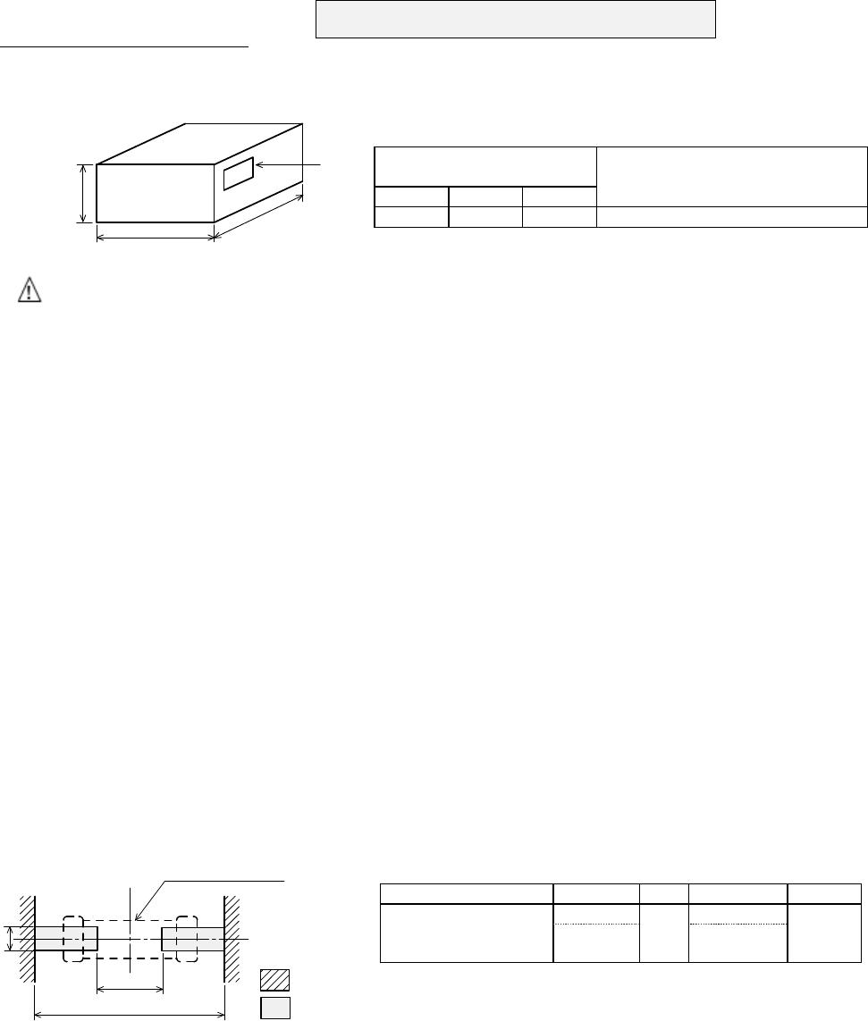
9-3.Reworking with soldering iron
Pre-heating: 150°C, 1 min Soldering iron output: 80W max.
Tip temperature: 350°C max. Tip diameter:φ3mm max.
Soldering time : 3(+1,-0) seconds. Times : 2times max.
Note :Do not directly touch the products with the tip of the soldering iron in order to prevent the crack
on the ferrite material due to the thermal shock.
9-4.Solder Volume
Solder shall be used not to be exceeded as shown below.
1/3TtT
(T:Chip thickness)
Accordingly increasing the solder volume, the mechanical stress to product is also increased.
Exceeding solder volume may cause the failure of mechanical or electrical performance.
9-5.Attention regarding P.C.B. bending
The following shall be considered when designing and laying out P.C.B.'s.
(1) P.C.B. shall be designed so that products are not subject to the mechanical stress for board warpage.
<Products direction>
Products shall be located in the sideways
direction (Length:a<b) to the mechanical
stress.
(2)Products location on P.C.B. separation.
Products (A,B,C,D) shall be located carefully
so that products are not subject to the
mechanical stress due to warping the board.
Because they may be subjected the mechanical
stress in order of A>C>B D.
9-6.Mounting density
Add special attention to radiating heat of products when mounting the inductor near the products with heating.
The excessive heat by other products may cause deterioration at joint of this product with substrate.
Recommendable
Upper Limit
t
Poor example
Good example
b
a
Seam
Slit
A
D
B
C
b
a
Length:a
<
b
Limit Profile
Standard Profile
90s±30s
230℃
260
245℃±3
220℃
30s~60s
60s max.
180
150
Temp.
(s)
(℃)
Time.

BLM18SG121TZ1D

Mfr. #:
Manufacturer:
Murata Electronics
Description:
Ferrite Beads 0603 120ohms 1000mA Auto Infotainment
Lifecycle:
New from this manufacturer.
Delivery:
DHL FedEx Ups TNT EMS
Payment:
T/T Paypal Visa MoneyGram Western Union