Specifications subject to change without notice. All dimensions in inches. © Copyright 2012 The Connor-Winfield Corporation
2111 Comprehensive Drive
Aurora, Illinois 60505
Phone: 630-851-4722
Fax: 630- 851- 5040
www.conwin.com
2111 Comprehensive Drive
Aurora, Illinois 60505
Phone: 630-851-4722
Fax: 630- 851- 5040
www.conwin.com
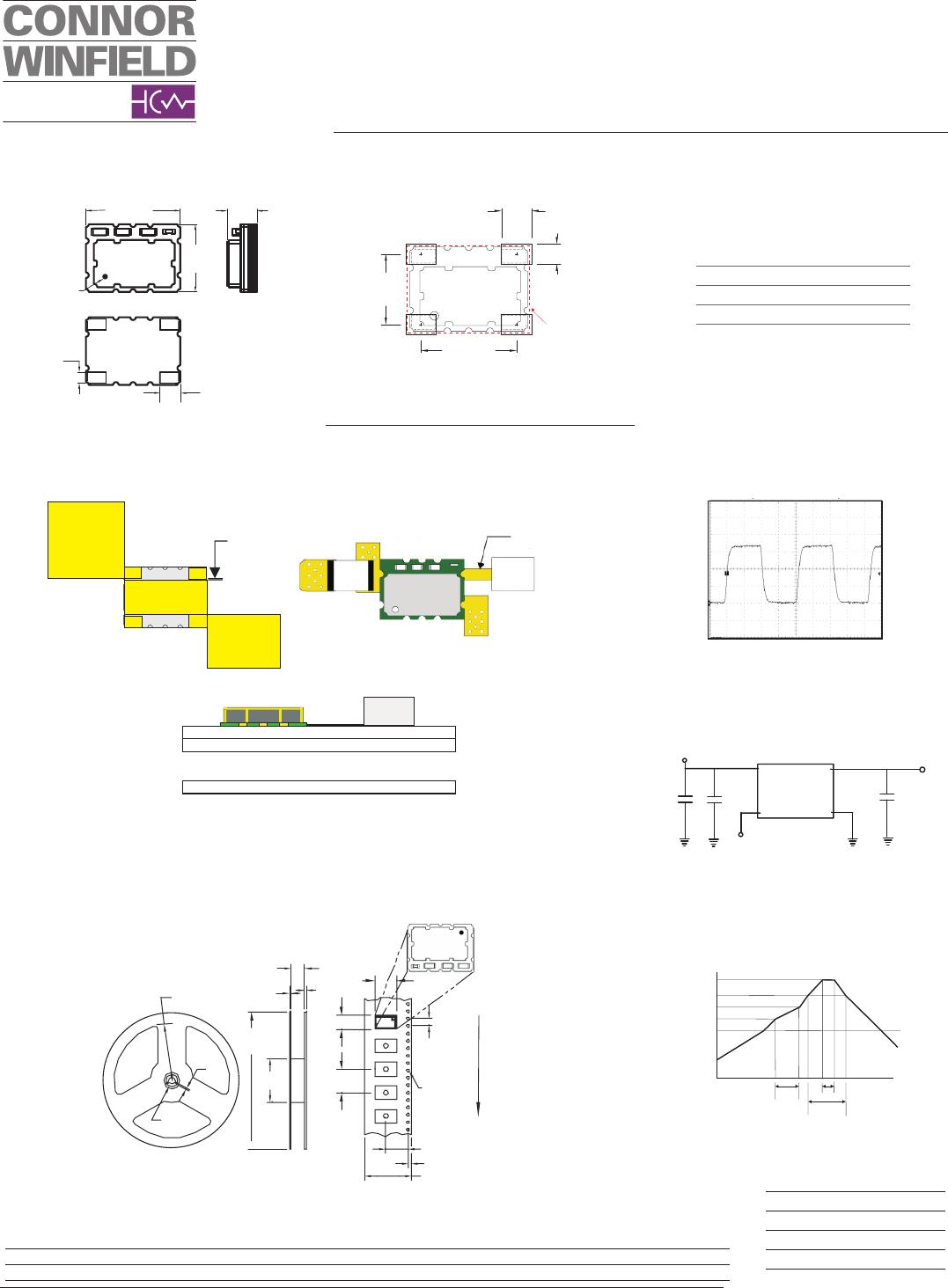
5x7mm
Precision TCXO
In Stock at Digi-Key
Description:
The Connor-Winfield’s DV75C is a
5x7mm Surface Mount Temperature
Compensated Crystal Controlled
Oscillator (TCXO) with LVCMOS output.
Through the use of Analog Temperature
Compensation the DV75C is capable of
holding sub 1-ppm stabilities over the -40
to 85°C temperature range. The DV75C
meets STRATUM 3 requirements.
Operating Specifications
Parameter Minimum Nominal Maximum Units Notes
Nominal Frequency (Fo) - 10.0, 12.8 or 20.0 - MHz
Frequency Calibration @ 25 °C -1.0 - 1.0 ppm 1
Frequency Stability vs. Temperature -0.28 - 0.28 ppm 2
Holdover Stability (Over 24 Hours) -0.32 - 0.32 ppm 3
Frequency vs. Load Stability -0.20 - 0.20 ppm ±5%
Frequency vs. Voltage Stability -0.20 - 0.20 ppm ±5%
Static Temperature Hysteresis - - 0.4 ppm Absolute, 4
Total Frequency Tolerance: -4.6 - 4.6 ppm 5
Operating Temperature Range: -40 - 85 °C
Supply Voltage (Vcc) 3.135 3.3 3.465 Vdc ±5%
Supply Current (Icc) - - 6 mA
Period Jitter - 3 5 ps rms
Integrated Phase Jitter - 0.5 1.0 ps rms 6
Typical Phase Noise Fo = 10.0 MHz
SSB Phase Noise at 10Hz offset - -80 - dBc/Hz
SSB Phase Noise at 100Hz offset - -110 - dBc/Hz
SSB Phase Noise at 1KHz offset - -135 - dBc/Hz
SSB Phase Noise at 10KHz offset - -150 - dBc/Hz
SSB Phase Noise at 100KHz offset - -150 - dBc/Hz
Start-up Time - - 5 ms
Absolute Maximum Ratings
Parameter Minimum Nominal Maximum Units Notes
Storage Temperature -55 - 85 °C
Supply Voltage (Vcc) -0.5 - 6.0 Vdc
Input Voltage -0.5 - Vcc+0.5 Vdc
US Headquarters:
630-851-4722
European Headquarters:
+353-61-472221
LVCMOS Output Characteristics
Parameter Minimum Nominal Maximum Units Notes
Load - 15 - pF 7
Voltage (High) (Voh) 90%Vcc - - Vdc
(Low) (Vol) - - 10%Vcc Vdc
Duty Cycle at 50% of Vcc 45 50 55 %
Rise / Fall Time 10% to 90% - - 8 ns
Package Characteristics
Package Hermetically sealed crystal mounted on a ceramic package
Ordering Information
DV75C-010.0M*, DV75C-012.8M*or DV75C-020.0M*
* For the tape and reel option, add -T to the end of the part number. Example: DV75C-010.0M-T
DV75C 1202
12.8 MHZ
Bulletin
Tx355
Page
1 of 3
Revision
02
Date
15 Apr 2013
Environmental Characteristics
Vibration: Vibration per Mil Std 883E Method 2007.3 Test Condition A
Shock: Mechanical Shock per Mil Std 883E Method 2002.4 Test Condition B.
Soldering Process; RoHS compliant lead free. See soldering profile on page 2.
Features:
Model: DV75C
3.3 Vdc Operation
LVCMOS Output
Frequency Stability: ± 0.28 ppm
Temperature Range: -40 to 85°C
Low Jitter <1ps RMS
5x7mm Surface Mount Package
Tape and Reel Packaging
RoHS Compliant / Pb Free
Applications:
• IEEE 1588 Applications
• Synchronous Ethernet slave clocks, ITU-T G.8262 EEC options 1 & 2
• Compliant to Stratum 3, GR-1244-CORE, GR-253-CORE & ITU-T-G.812 Type IV
• Wireless Communications
• Small Cells
• Test and Measurement