ADM810RARTZ-REEL7

ADM803/ADM809/ADM810 Data Sheet
ABSOLUTE MAXIMUM RATINGS
T
A
= 25°C, unless otherwise noted.
Table 2.
Parameter Ratings
V
CC
−0.3 V to +6 V
RESET,
RESET
(Push-Pull) −0.3 V to V
CC
+ 0.5 V
RESET (Open-Drain) −0.3 V to +6.0 V
Input Current
V
CC
20 mA
Output Current
RESET,
RESET
20 mA
Rate of Rise, V
CC
100 V/μs
θ
JA
Thermal Impedance
SC70 146°C/W
SOT-23 270°C/W
Lead Temperature (Soldering, 10 sec) 300°C
Vapor Phase (60 sec)
215°C
Infrared (15 sec) 220°C
Storage Temperature Range −65°C to +150°C
Stresses at or above those listed under Absolute Maximum
Ratings may cause permanent damage to the product. This is a
stress rating only; functional operation of the product at these
or any other conditions above those indicated in the operational
section of this specification is not implied. Operation beyond
the maximum operating conditions for extended periods may
affect product reliability.
Table 3. Reset Threshold Options
RESET Model Threshold (V)
ADM8xxL 4.63
ADM8xxM
4.38
ADM8xxJ (ADM809/ADM810 Only) 4.00
ADM8xxT 3.08
ADM8xxS 2.93
ADM8xxR 2.63
ADM8xxZ 2.32
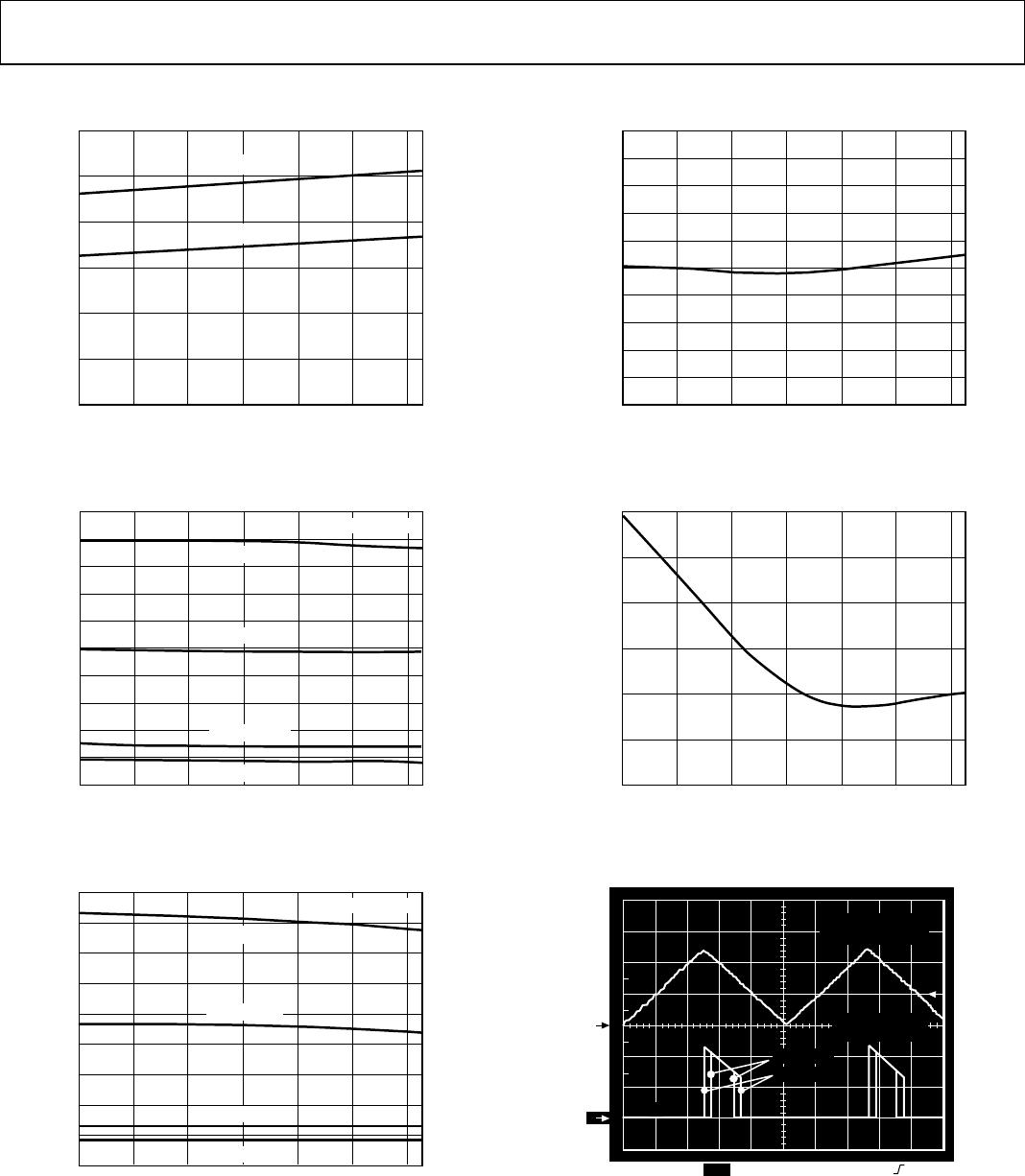
Figure 2. Power Fail Reset Timing
ESD CAUTION
t
1
t
1
V
REF
V
REF
V
REF
V
REF
V
CC
t
1 = RESET TIME = 240ms TYP
V
REF
= RESET VOLTAGE THRESHOLD
RESET
03736-003
Rev. I | Page 4 of 11
Data Sheet ADM803/ADM809/ADM810
PIN CONFIGURATIONS AND FUNCTION DESCRIPTIONS
Figure 3. ADM803/ADM809 Pin Configuration
Figure 4. ADM810 Pin Configuration
Table 4. Pin Function Descriptions
Pin No.
Mnemonic Description ADM803/ADM809 ADM810
1 1 GND Ground Reference for All Signals; 0 V.
N/A 2 RESET Active High Logic Output. RESET remains high while V
CC
is below the reset threshold
and remains high for 240 ms (typical) after V
CC
rises above the reset threshold.
2 N/A
RESET
Active Low Logic Output.
RESET
remains low while V
CC
is below the reset threshold
and remains low for 240 ms (typical) after V
CC
rises above the reset threshold.
3 3 V
CC
Supply Voltage Being Monitored.
GND
1
2
3
ADM803/
ADM809/
TOP VIEW
(Not to Scale)
V
CC
RESET
03736-002
GND
1
2
3
ADM810
TOP VIEW
(Not to Scale)
V
CC
RESET
03736-102
Rev. I | Page 5 of 11
ADM803/ADM809/ADM810 Data Sheet
TYPICAL PERFORMANCE CHARACTERISTICS
Figure 5. Supply Current vs. Temperature (No Load)
Figure 6. Power-Down Reset Delay vs. Temperature, ADM8xxL/M/J
Figure 7. Power-Down Reset Delay vs. Temperature, ADM8xxT/S/R/Z
Figure 8. Power-Up Reset Timeout vs. Temperature, ADM8xxR
Figure 9. Normalized Reset Voltage Threshold vs. Temperature
Figure 10. Reset Output Voltage vs. Supply Voltage
25
30
20
15
10
5
0
SUPPLY CURRENT (µA)
TEMPERATURE (°C)
–40 –20
0
20
40
60 80 85
03736-004
V
CC
= 5V
V
CC
= 3V
200
–40 –20 0
20
40 60 80
85
180
160
140
120
100
80
60
40
20
0
POWER-DOWN RESET (µs)
TEMPERATURE (°C)
V
OD
= V
TH
– V
CC
V
OD
= 10mV
V
OD
= 20mV
V
OD
= 100mV
V
OD
= 200mV
03736-005
180
160
140
120
100
80
60
40
20
0
POWER-DOWN RESET (µs)
V
OD
= V
TH
– V
CC
V
OD
= 10mV
V
OD
= 20mV
V
OD
= 100mV
V
OD
= 200mV
–40 –20 0 20 40 60 80 85
TEMPERATURE (°C)
03736-006
240.0
235.0
235.5
236.0
236.5
237.0
237.5
238.0
238.5
239.0
239.5
POWER-UP RESET TIMEOUT (ms)
–40
–20 0 20 40 60 80 85
TEMPERATURE (°C)
03736-007
1.0020
0.9990
1.0015
1.0010
1.0005
1.0000
0.9995
NORMALIZED RESET THRESHOLD
–40 –20
0 20 40
60 80 85
TEMPERATURE (°C)
03736-008
2
1
CH1
2.00V CH2
2.00V M 200ms
CH1
2.00V
T
T
SUPPLYVOLTAGE
5V p-p
RESET OUTPUT
VOLTAGE
ADM809T
ADM809R
03736-009
Rev. I | Page 6 of 11

ADM810RARTZ-REEL7

Mfr. #:
Manufacturer:
Analog Devices Inc.
Description:
Supervisory Circuits RESET GENERATORS I.C.
Lifecycle:
New from this manufacturer.
Delivery:
DHL FedEx Ups TNT EMS
Payment:
T/T Paypal Visa MoneyGram Western Union