UC3842A, UC3843A, UC2842A, UC2843A
http://onsemi.com
10
PIN FUNCTION DESCRIPTION
Pin
Function Description
8−Pin 14−Pin
1 1 Compensation This pin is Error Amplifier output and is made available for loop compensation.
2 3 Voltage
Feedback
This is the inverting input of the Error Amplifier. It is normally connected to the switching pow-
er supply output through a resistor divider.
3 5 Current Sense A voltage proportional to inductor current is connected to this input. The PWM uses this infor-
mation to terminate the output switch conduction.
4 7 R
T
/C
T
The Oscillator frequency and maximum Output duty cycle are programmed by connecting
resistor R
T
to V
ref
and capacitor C
T
to ground. Operation to 500 kHz is possible.
5 GND This pin is the combined control circuitry and power ground (8−pin package only).
6 10 Output This output directly drives the gate of a power MOSFET. Peak currents up to 1.0 A are
sourced and sunk by this pin.
7 12 V
CC
This pin is the positive supply of the control IC.
8 14 V
ref
This is the reference output. It provides charging current for capacitor C
T
through
resistor R
T
.
8 Power Ground This pin is a separate power ground return (14−pin package only) that is connected back
to the power source. It is used to reduce the effects of switching transient noise on the control
circuitry.
11 V
C
The Output high state (V
OH
) is set by the voltage applied to this pin (14−pin package only).
With a separate power source connection, it can reduce the effects of switching transient
noise on the control circuitry.
9 GND This pin is the control circuitry ground return (14−pin package only) and is connected back to
the power source ground.
2,4,6,13 NC No connection (14−pin package only). These pins are not internally connected.
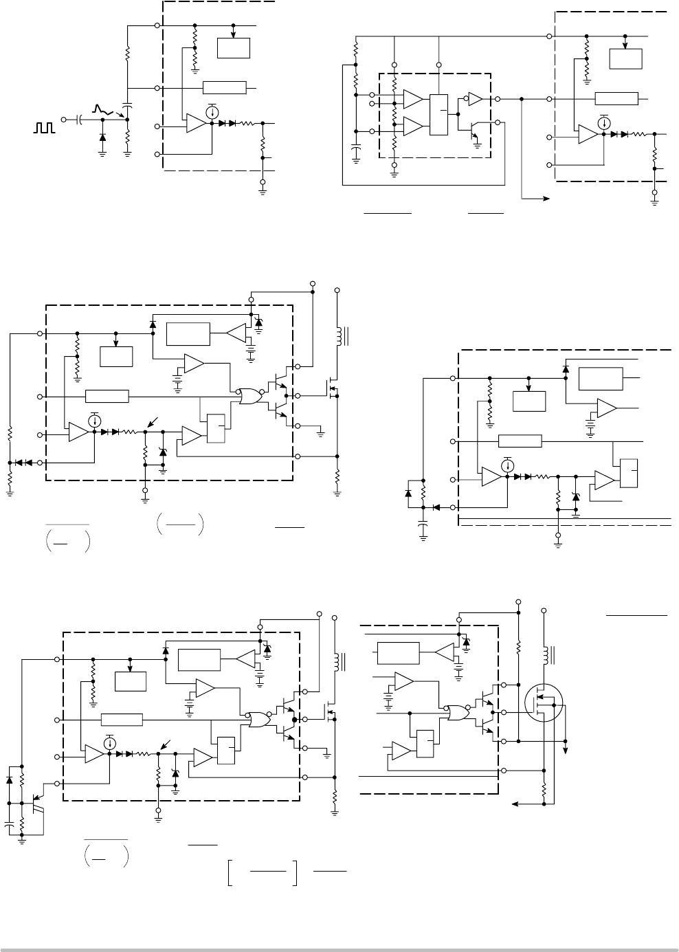
Undervoltage Lockout
Two undervoltage lockout comparators have been
incorporated to guarantee that the IC is fully functional
before the output stage is enabled. The positive power
supply terminal (V
CC
) and the reference output (V
ref
) are
each monitored by separate comparators. Each has built−in
hysteresis to prevent erratic output behavior as their
respective thresholds are crossed. The V
CC
comparator
upper and lower thresholds are 16 V/10 V for the UCX842A,
and 8.4 V/7.6 V for the UCX843A. The V
ref
comparator
upper and lower thresholds are 3.6V/3.4 V. The large
hysteresis and low startup current of the UCX842A makes
it ideally suited in off−line converter applications where
efficient bootstrap startup techniques are required
(Figure 34). The UCX843A is intended for lower voltage dc
to dc converter applications. A 36 V zener is connected as
a shunt regulator form V
CC
to ground. Its purpose is to
protect the IC from excessive voltage that can occur during
system startup. The minimum operating voltage for the
UCX842A is 11 V and 8.2 V for the UCX843A.
Output
These devices contain a single totem pole output stage that
was specifically designed for direct drive of power
MOSFETs. It is capable of up to ±1.0 A peak drive current
and has a typical rise and fall time of 50 ns with a 1.0 nF load.
Additional internal circuitry has been added to keep the
Output in a sinking mode whenever an undervoltage lockout
is active. This characteristic eliminates the need for an
external pull−down resistor.
The SOIC−14 surface mount package provides separate
pins for V
C
(output supply) and Power Ground. Proper
implementation will significantly reduce the level of
switching transient noise imposed on the control circuitry.
This becomes particularly useful when reducing the I
pk(max)
clamp level. The separate V
C
supply input allows the
designer added flexibility in tailoring the drive voltage
independent of V
CC
. A zener clamp is typically connected
to this input when driving power MOSFETs in systems
where V
CC
is greater than 20 V. Figure 26 shows proper
power and control ground connections in a current sensing
power MOSFET application.
Reference
The 5.0 V bandgap reference is trimmed to ±1.0%
tolerance at T
J
= 25°C on the UC284XA, and ± 2.0% on the
UC384XA. Its primary purpose is to supply charging current
to the oscillator timing capacitor. The reference has short
circuit protection and is capable of providing in excess of
20 mA for powering additional control system circuitry.
UC3842A, UC3843A, UC2842A, UC2843A
http://onsemi.com
11
DESIGN CONSIDERATIONS
Do not attempt to construct the converter on
wire−wrap or plug−in prototype boards. High Frequency
circuit layout techniques are imperative to prevent pulse
width jitter. This is usually caused by excessive noise
pick−up imposed on the Current Sense or Voltage Feedback
inputs. Noise immunity can be improved by lowering circuit
impedances at these points. The printed circuit layout should
contain a ground plane with low−current signal and
high−current switch and output grounds returning on
separate paths back to the input filter capacitor. Ceramic
bypass capacitors (0.1 F) connected directly to V
CC
, V
C
,
and V
ref
may be required depending upon circuit layout.
This provides a low impedance path for filtering the high
frequency noise. All high current loops should be kept as
short as possible using heavy copper runs to minimize
radiated EMI. The Error Amp compensation circuitry and
the converter output voltage divider should be located close
to the IC and as far as possible from the power switch and
other noise generating components.
Current mode converters can exhibit subharmonic
oscillations when operating at a duty cycle greater than 50%
with continuous inductor current. This instability is
independent of the regulators closed−loop characteristics
and is caused by the simultaneous operating conditions of
fixed frequency and peak current detecting. Figure 20A
shows the phenomenon graphically. At t
0
, switch
conduction begins, causing the inductor current to rise at a
slope of m
1
. This slope is a function of the input voltage
divided by the inductance. At t
1
, the Current Sense Input
reaches the threshold established by the control voltage.
This causes the switch to turn off and the current to decay at
a slope of m
2
until the next oscillator cycle. The unstable
condition can be shown if a perturbation is added to the
control voltage, resulting in a small I (dashed line). With
a fixed oscillator period, the current decay time is reduced,
and the minimum current at switch turn−on (t
2
) is increased
by I + I m2/m1. The minimum current at the next cycle
(t
3
) decreases to (I +
I m
2
/m
1
) (m
2
/m
1
). This perturbation
is multiplied by m
2
.m
1
on each succeeding cycle, alternately
increasing and decreasing the inductor current at switch
turn−on. Several oscillator cycles may be required before
the inductor current reaches zero causing the process to
commence again. If m
2
/m
1
is greater than 1, the converter
will be unstable. Figure 20B shows that by adding an
artificial ramp that is synchronized with the PWM clock to
the control voltage, the I perturbation will decrease to zero
on succeeding cycles. This compensation ramp (m
3
) must
have a slope equal to or slightly greater than m
2
/2 for
stability. With m
2
/2 slope compensation, the average
inductor current follows the control voltage yielding true
current mode operation. The compensating ramp can be
derived from the oscillator and added to either the Voltage
Feedback or Current Sense inputs (Figure 33).
Figure 20. Continuous Current Waveforms
(A)
(B)
t
0
t
1
t
2
t
3
t
4
t
5
t
6
Control Voltage
I
m1
m2
m3
m1
m2
Oscillator Period
Oscillator Period
Control Voltage
I
Inductor
Current
I + I
m
2
m
1
m
2
m
1
I + I
m
2
m
1
Inductor
Current
UC3842A, UC3843A, UC2842A, UC2843A
http://onsemi.com
12
Figure 21. External Clock Synchronization
Figure 22. External Duty Cycle Clamp and
Multi Unit Synchronization
Figure 23. Adjustable Reduction of Clamp Level Figure 24. Soft−Start Circuit
Figure 25. Adjustable Buffered Reduction of
Clamp Level with Soft−Start
Figure 26. Current Sensing Power MOSFET
Virtually lossless current sensing can be achieved with the implementation of a
SENSEFET power switch. For proper operation during over current conditions, a
reduction of the I
pk(max)
clamp level must be implemented. Refer to Figures 23 and 25.
The diode clamp is required if the Sync amplitude is large enough to
cause the bottom side of CT to go more than 300 mV below ground.
External
Sync
Input
47
5(9)
R
R
Bias
Osc
V
ref
R
T
8(14)
4(7)
2(3)
1(1)
0.01
C
T
2R
R
EA
+
+
5(9)
R
R
Bias
Osc
8(14)
4(7)
2(3)
1(1)
2R
R
EA
+
+
7
5.0k
3
8
6
5
1
C
R
S
MC1455
2
R
A
+
+
4
Q
5.0k
5.0k
R
B
To
Additional
UCX84XA’s
f =
1.44
(R
A
+ 2R
B
)C
D
max
=
R
B
R
A
+ 2R
B
5(9)
R
R
Bias
Osc
8(14)
4(7)
2(3)
1(1)
2R
R
EA
+
+
Q1
R
S
3(5)
5(8)
1.0V
R
S
Q
Comp/Latch
5.0V
ref
V
Clamp
V
in
V
CC
7(11)
6(10)
+
+
+
+
7(12)
+
R
1
R
2
R
2
V
Clamp
=
1.67
+ 1
+ 0.33 x 10 − 3I
pk(max)
=
VClamp
RS
Where: 0 V
Clamp
1.0 V
R2
R1
1.0mA
R
1
R
1
+ R
2
5(9)
R
R
Bias
Osc
8(14)
4(7)
2(3)
1(1)
2R
R
EA
+
+
1.0V
R
S
Q
5.0V
ref
+
+
+
C
t
Soft−Start
3600C in F
1.0M
1.0mA
5(9)
R
R
Bias
Osc
8(14)
4(7)
2(3)
1(1)
2R
R
EA
+
+
Q1
R
S
3(5)
5(8)
1.0V
R
S
Q
Comp/Latch
5.0V
ref
V
Clamp
V
in
V
CC
7(11)
6(10)
+
+
+
+
7(12)
+
MPSA63
R1
R2
C
t
Softstart
= − In 1 −
V
C
R
1
R
2
C
R
2
V
Clamp
=
1.67
+ 1
I
pk(max)
=
VClamp
RS
Where: 0 V
Clamp
1.0 V
1.0mA
R
1
3V
Clamp
R
1
+ R
2
R
S
1/4
W
(5)
(8)
R
S
Q
Comp/Latch
5.0V
ref
V
in
V
CC
(11)
(10)
+
+
+
+
(12)
+
Power Ground
To Input Source
Return
V
Pin
5 =
If: SENSEFET = MTP10N10M
R
S
= 200
Then: V
pin
5 = 0.075 I
pk
SENSEFET
R
S
I
pk
r
DS(on)
M
G
D
S
K
Control CIrcuitry
Ground:
To Pin (9)
r
DM(on)
+ R
S

UC3842ANG

Mfr. #:
Manufacturer:
ON Semiconductor
Description:
Switching Controllers 52kHz 1A Current PWM w/96% Duty Cycle Max
Lifecycle:
New from this manufacturer.
Delivery:
DHL FedEx Ups TNT EMS
Payment:
T/T Paypal Visa MoneyGram Western Union