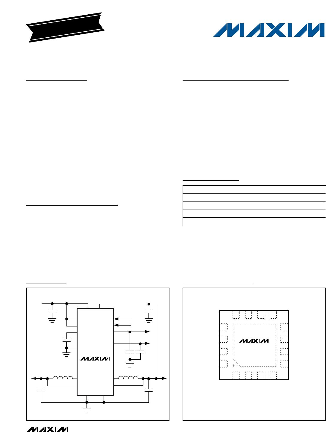
General Description
The MAX8667/MAX8668 dual step-down converters
with dual low-dropout (LDO) linear regulators are
intended to power low-voltage microprocessors or
DSPs in portable devices. They feature high efficiency
with small external component size. The step-down
converters are adjustable from 0.6V to 3.3V (MAX8668)
or factory preset (MAX8667) with guaranteed output
current of 600mA for OUT1 and 1200mA for OUT2. The
1.5MHz hysteretic-PWM control scheme allows for tiny
external components and reduces no-load operating
current to 100µA with all outputs enabled. Dual low-qui-
escent-current, low-noise LDOs operate down to 1.7V
supply voltage. The MAX8667/MAX8668 have individ-
ual enables for each output, maximizing flexibility.
The MAX8667/MAX8668 are available in the space-
saving, 3mm x 3mm, 16-pin thin QFN package.
Applications
Cell Phones/Smartphones
PDA and Palmtop Computers
Portable MP3 and DVD Players
Digital Cameras, Camcorders
PCMCIA Cards
Handheld Instruments
Features
o Tiny, Thin QFN 3mm x 3mm Package
o Individual Enables
o Step-Down Converters
600mA Guaranteed Output Current on OUT1
1200mA Guaranteed Output Current on OUT2
Tiny Size 2.2µH Chip Inductor (0805)
Output Voltage from 0.6V to 3.3V (MAX8668)
Ultra-Fast Line and Load Transients
Low 25µA Supply Current Each
o LDOs
300mA Guaranteed
Low 1.7V Minimum Supply Voltage
Low Output Noise
MAX8667/MAX8668
1.5MHz Dual Step-Down DC-DC Converters
with Dual LDOs and Individual Enables
________________________________________________________________
Maxim Integrated Products
1
15
16
14
13
5
6
7
IN34
OUT4
8
EN3
LX2
PGND2
LX1
13
OUT1 (FB1)
4
12 10 9
EN1
EN2
OUT2 (FB2)
REF
GND
EN4
MAX8667
MAX8668
OUT3 IN12
2
11
PGND1
THIN QFN
(3mm x 3mm)
TOP VIEW
( ) ARE FOR THE MAX8668
Pin Configuration
IN34
LX2
LX1
OUT2
OUT1
2.6V TO 5.5V
OUT3
OUT4
REF
GND
IN12
300mA
300mA
EN1
EN2
EN3
EN4
600mA
1.2A
PGND1 PGND2
10µF 4.7µF
4.7µF
4.7µF
0.01µF
2.2µH
2.2µH
2.2µF
2.2µF
MAX8667
Typical Operating Circuit
19-0784; Rev 1; 7/07
For pricing, delivery, and ordering information, please contact Maxim/Dallas Direct! at
1-888-629-4642, or visit Maxim’s website at www.maxim-ic.com.
EVALUATION KIT
AVAILABLE
Ordering Information continued at the end of data sheet.
Selector Guide appears at the end of data sheet.
Ordering Information
Note: All MAX8667/MAX8668 parts are in a 16-pin, thin QFN,
3mm x 3mm package and operate in the -40°C to +85°C
extended temperature range.
+
Denotes a lead-free package.
PART PKG CODE TOP MARK
MAX8667ETEAA+
T1633-4 AEQ
MAX8667ETEAB+
T1633-4 AFI
MAX8667ETEAC+
T1633-4 AFM
MAX8667ETECQ+
T1633-4 AFN
MAX8667/MAX8668
1.5MHz Dual Step-Down DC-DC Converters
with Dual LDOs and Individual Enables
2 _______________________________________________________________________________________
ABSOLUTE MAXIMUM RATINGS
ELECTRICAL CHARACTERISTICS
(V
IN34
= V
IN12
= 3.6V, T
A
= -40°C to +85°C, unless otherwise noted. Typical values are at T
A
= +25°C.) (Note 1)
Stresses beyond those listed under “Absolute Maximum Ratings” may cause permanent damage to the device. These are stress ratings only, and functional
operation of the device at these or any other conditions beyond those indicated in the operational sections of the specifications is not implied. Exposure to
absolute maximum rating conditions for extended periods may affect device reliability.
IN12, IN34, FB1, FB2, EN1, EN2, EN3, EN4, OUT1,
OUT2, REF to GND............................................-0.3V to +6.0V
OUT3,
OUT4 to GND.....-0.3V to the lesser of + 6V or (V
IN34
+ 0.3V)
PGND1, PGND2 to GND .......................................-0.3V to +0.3V
LX1, LX2 Current ..........................................................1.5A RMS
LX1, LX2 to GND (Note 1) .......................-0.3V to (V
IN12
+ 0.3V)
Continuous Power Dissipation (T
A
= +70°C)
16-Pin, 3mm x 3mm Thin QFN
(derate 20.8mW/°C above +70°C).............................1667mW
Operating Temperature Range ...........................-40°C to +85°C
Junction Temperature..................................................... +150°C
Storage Temperature Range .............................-65°C to +150°C
Lead Temperature (soldering, 10s) .................................+300°C
PARAMETER CONDITIONS MIN TYP MAX UNITS
IN34 Supply Range V
IN12
V
IN34
1.7 5.5 V
IN12 Supply Range MAX8668, V
IN12
V
IN34
2.6 5.5 V
IN12 Suppy Range MAX8667, V
IN12
V
IN34
2.8 5.5 V
T
A
= +25°C 1 µA
Shutdown Supply Current,
I
IN12
+ I
IN34
V
IN12
= V
IN34
= 4.2V V
EN_
= 0V
T
A
= +85°C 0.05 µA
No Load Supply Current,
I
IN12
+ I
IN34
MAX8667ETEJS+, all regulators enabled 100 150 µA
UNDERVOLTAGE LOCKOUT
V
IN12
rising 2.4 2.5 2.6 V
IN12 UVLO
V
IN12
hysteresis 0.1 V
V
IN34
rising 1.5 1.6 1.7 V
IN34 UVLO
V
IN34
hysteresis 0.1 V
THERMAL SHUTDOWN
Threshold T
A
rising +160 °C
Hysteresis 15 °C
REFERENCE
Reference Bypass Output
Voltage
0.591 0.600 0.609 V
REF Supply Rejection 2.6V (V
IN12
= V
IN34
) 5.5V 0.15 mV/V
LOGIC AND CONTROL INPUTS
EN_ Input Low Level
1.7V V
IN34
5.5V
2.6V V
IN12
5.5V
0.4 V
EN_ Input High Level
1.7V V
IN34
5.5V
2.6V V
IN12
5.5V
1.44 V
T
A
= +25°C -1 +1
EN_ Input Leakage Current V
IN12
= V
IN34
= 5.5V
T
A
= +85°C 0.001
µA
STEP-DOWN CONVERTERS
Minimum Adjustable Output
Voltage
MAX8668 0.6 V
Note 1: LX_ has internal clamp diodes to GND and IN12. Applications that forward bias these diodes should take care not to exceed
the IC’s package-dissipation limits.
MAX8667/MAX8668
1.5MHz Dual Step-Down DC-DC Converters
with Dual LDOs and Individual Enables
_______________________________________________________________________________________ 3
Note 1: All devices are 100% production tested at T
A
= +25°C. Limits over the operating temperature range are guaranteed by design.
PARAMETER CONDITIONS MIN TYP MAX UNITS
Maximum Adjustable Output
Voltage
MAX8668 3.3 V
T
A
= +25°C 0.588 0.600 0.612
FB1, FB2 Regulation Voltage
MAX8668, no load,
V
FB_
falling
T
A
= -40°C to +85°C 0.582 0.600 0.618
V
T
A
= +25°C 1.274 1.300 1.326
OUT1, OUT2 Regulation Voltage
MAX8667ETEJS+, no load, V
OUT_
falling
T
A
= -40°C to +85°C 1.261 1.300 1.339
V
FB1, FB2 Line Regulation MAX8668, V
IN12
= 2.6V to 5.5V 0.01 %/V
OUT1, OUT2 Line Regulation MAX8667, V
IN12
= 2.8V to 5.5V 0.05 %/V
MAX8668, shutdown mode 0.1
FB1, FB2 Bias Current
MAX8668, V
FB1
= 0.5V 0.01
µA
pMOSFET switch (I
LIMP1
) 700 900 1100
OUT1 Current Limit
nMOSFET rectifier (valley current) 500 750 1000
mA
pMOSFET switch (I
LIMP2
) 1333 1667 2000
OUT2 Current Limit
nMOSFET rectifier (valley current) 1200 1500 1800
mA
pMOSFET switch, I
LX1
= -400mA 0.3 0.6
OUT1 On-Resistance
nMOSFET rectifier, I
LX1
= 400mA 0.3 0.6
pMOSFET switch, I
LX2
= -400mA 0.12 0.27
OUT2 On-Resistance
nMOSFET rectifier, I
LX2
= 400mA 0.12 0.27
Rectifier-Off Current Threshold
(I
LXOFF
)
60 120 mA
T
A
= +25°C -1 +1
LX Leakage Current LX_ = 5.5V
T
A
= +85°C 0.1
µA
Minimum On-Time 100 ns
Minimum Off-Time 50 ns
LDO REGULATORS
Supply Current Each LDO 20 µA
1mA load, T
A
= +25°C -1.5 +1.5
Output-Voltage Accuracy
1mA to 300mA load -3.0 +3.0
%
Line Regulation V
IN34
= 3.6V to 5.5V, 1mA load 0.003 %/V
Dropout Voltage V
IN34
= 1.8V, 300mA load 130 250 mV
Current Limit V
OUT3
, V
OUT4
90% of nominal value 375 420 465 mA
Soft-Start Ramp Time To 90% of final value 0.1 ms
Output Noise 100Hz to 100kHz, 30mA load, V
OUT3
and V
OUT4
= 2.8V 75 µV
RMS
Power-Supply Rejection Ratio f < 1kHz, 30mA load 57 dB
Shutdown Output Resistance 1k
TIMING (See Figure 2)
OUT1, OUT2 25
Power-On Time (t
PWRON
)
OUT3, OUT4 45
µs
OUT1, OUT2 15
Enable Time (t
EN
)
OUT3, OUT4 35
µs
ELECTRICAL CHARACTERISTICS (continued)
(V
IN34
= V
IN12
= 3.6V, T
A
= -40°C to +85°C, unless otherwise noted. Typical values are at T
A
= +25°C.) (Note 1)

MAX8668ETEX+

Mfr. #:
Manufacturer:
Maxim Integrated
Description:
Voltage Regulators - Switching Regulators 1.5MHz Dl Step-Down DC/DC Converte
Lifecycle:
New from this manufacturer.
Delivery:
DHL FedEx Ups TNT EMS
Payment:
T/T Paypal Visa MoneyGram Western Union