2DA1797-13

2DA1797
Document number: DS31619 Rev. 4 - 2
1 of 7
www.diodes.com
November 2013
© Diodes Incorporated
2D
A
1797
NEW PRODUCT
50V PNP SURFACE MOUNT TRANSISTOR
Features
Epitaxial Planar Die Construction
Ideally Suited for Automated Assembly Processes
Ideal for Medium Power Switching or Amplification Applications
Complementary NPN Type Available (2DC4672)
Totally Lead-Free & Fully RoHS compliant (Notes 1 & 2)
Halogen and Antimony Free. “Green” Device (Note 3)
Qualified to AEC-Q101 Standards for High Reliability
PPAP Capable (Note 4)
Mechanical Data
Case: SOT89
Case Material: Molded Plastic, "Green” Molding Compound.
UL Flammability Classification Rating 94V-0
Moisture Sensitivity: Level 1 per J-STD-020
Terminals: Finish — Matte Tin. Solderable per MIL-STD-202,
Method 208
Weight: 0.052 grams (approximate)
Ordering Information (Notes 4 & 5)
Part Number Compliance Marking Reel size (inches) Tape width (mm) Quantity per reel
2DA1797-13 AEC-Q101 1797 13 12 2,500
2DA1797Q-13 Automotive 1797 13 12 2,500
Notes: 1. No purposely added lead. Fully EU Directive 2002/95/EC (RoHS) & 2011/65/EU (RoHS 2) compliant.
2. See http://www.diodes.com/quality/lead_free.html for more information about Diodes Incorporated’s definitions of Halogen- and Antimony-free, "Green"
and Lead-free.
3. Halogen- and Antimony-free "Green” products are defined as those which contain <900ppm bromine, <900ppm chlorine (<1500ppm total Br + Cl) and
<1000ppm antimony compounds.
4. Automotive products are AEC-Q101 qualified and are PPAP capable. Automotive, AEC-Q101 and standard products are electrically and thermally the
same, except where specified. For more information, please refer to http://www.diodes.com/quality/product_compliance_definitions/.
5. For packaging details, go to our website at http://www.diodes.com/products/packages.html.
Marking Information
Top View
SOT89
Device symbol
Top View
Pin-Out
1797 = Product Type Marking Code
YWW = Date Code Marking
Y = Last digit of year (ex: 8 = 2008)
WW = Week code (01 – 53)
1797
YWW
C
E
B
C
E
C
B
2DA1797
Document number: DS31619 Rev. 4 - 2
2 of 7
www.diodes.com
November 2013
© Diodes Incorporated
2D
A
1797
NEW PRODUCT
Absolute Maximum Ratings (@T
A
= +25°C, unless otherwise specified.)
Characteristic Symbol Value Unit
Collector-Base Voltage
V
CBO
-50 V
Collector-Emitter Voltage
V
CEO
-50 V
Emitter-Base Voltage
V
EBO
-6 V
Peak Pulse Current
I
CM
-6 A
Continuous Collector Current
I
C
-3 A
Thermal Characteristics (@T
A
= +25°C, unless otherwise specified.)
Characteristic Symbol Value Unit
Power Dissipation (Note 6)
P
D
0.9 W
Thermal Resistance, Junction to Ambient Air (Note 6)
R
JA
139 °C/W
Power Dissipation (Note 7)
P
D
2 W
Thermal Resistance, Junction to Ambient Air (Note 7)
R
JA
62.5 °C/W
Thermal Resistance, Junction to Lead (Note 8)
R
JL
5.3 °C/W
Operating and Storage Temperature Range
T
J
, T
STG
-55 to +150 °C
ESD Ratings (Note 9)
Characteristic Symbol Value Unit JEDEC Class
Electrostatic Discharge - Human Body Model ESD HBM 4,000 V 3A
Electrostatic Discharge - Machine Model ESD MM 400 V C
Notes: 6. Device mounted on FR-4 PCB with minimum recommended pad layout.
7. Device mounted on FR-4 PCB with 1 inch
2
copper pad layout.
8. Thermal resistance from junction to solder-point (on the exposed collector pad).
9. Refer to JEDEC specification JESD22-A114 and JESD22-A115.
2DA1797
Document number: DS31619 Rev. 4 - 2
3 of 7
www.diodes.com
November 2013
© Diodes Incorporated
2D
A
1797
NEW PRODUCT
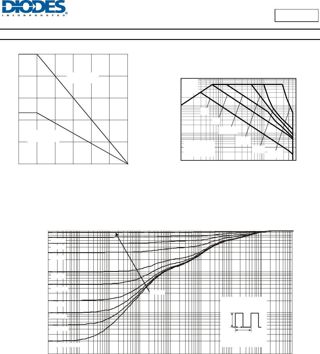
Thermal Characteristics and Derating Information (@T
A
= +25°C, unless otherwise specified.)
100m 1 10
10m
100m
1
10
100µs
Single Pulse
T
amb
=25°C
V
CE(sat)
Limited
1ms
10ms
100ms
1s
DC
Safe Operating Area
-I
C
Collector Current (A)
-V
CE
Collector-Emitter Voltage (V)
0
0.4
0.8
25 50
75
100 125
150
P
,
P
O
WE
R
DISSI
P
A
T
I
O
N (W)
D
T , AMBIENT TEMPERATURE (°C)
Fig. 1 Power Dissipation vs.
Ambient Temperature
A
1.2
1.6
2.0
0
FR-4 PCB
1 inch copper pad
2
FR-4 PCB
Minimum
recommended pad
0.00001 0.0001 0.001 0.01 0.1 1 10 100 1,000
Fig. 10 Transient Thermal Response
t , PULSE DURATION TIME (s)
1
0.001
0.01
0.1
1
r(t), TR
A
N
S
I
E
NT TH
E
R
M
A
L R
E
S
I
S
T
A
N
C
E
T - T = P * R (t)
Duty Cycle, D = t /t
JA JA
12
R (t) = r(t) *
JA
R
R = 126°C/W
JA
JA
P(pk)
t
1
t
2
D = 0.7
D = 0.3
D = 0.1
D = 0.05
D = 0.02
D = 0.01
D = 0.005
D = Single Pulse
D = 0.9
D = 0.5

2DA1797-13

Mfr. #:
Manufacturer:
Diodes Incorporated
Description:
Bipolar Transistors - BJT SMT 2.5K
Lifecycle:
New from this manufacturer.
Delivery:
DHL FedEx Ups TNT EMS
Payment:
T/T Paypal Visa MoneyGram Western Union

Products related to this Datasheet