LTC2607/LTC2617/LTC2627
10
26071727fa
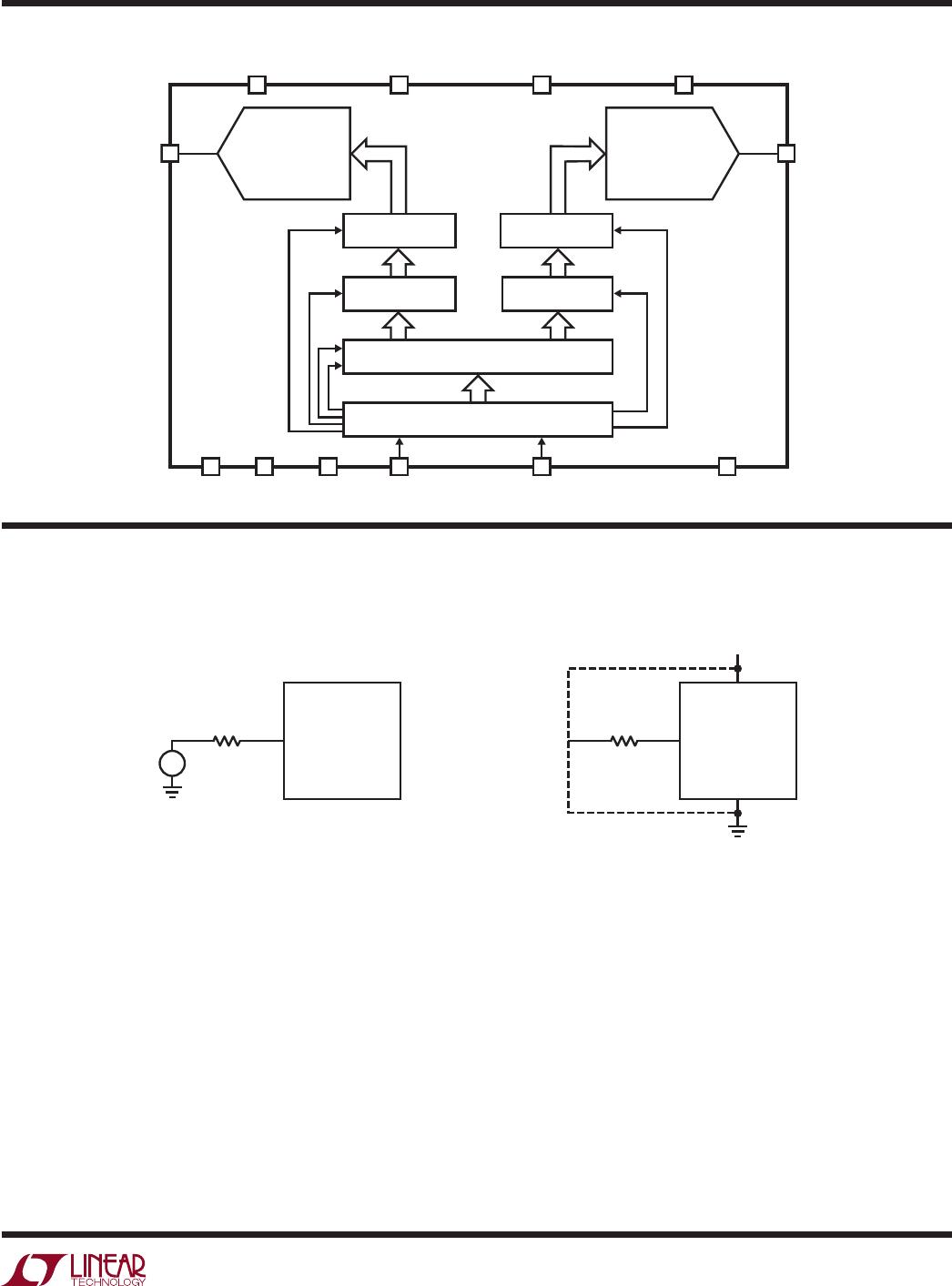
pin Functions
CA0 (Pin 1): Chip Address Bit 0. Tie this pin to V
CC
, GND
or leave it floating to select an I
2
C slave address for the
part (Table 1).
CA1 (Pin 2): Chip Address Bit 1. Tie this pin to V
CC
, GND
or leave it floating to select an I
2
C slave address for the
part (Table 1).
LDAC (Pin 3): Asynchronous DAC Update. A falling edge
of this input after four bytes have been written into the part
immediately updates the DAC register with the contents of
the input register. A low on this input without a complete
32-bit (four bytes including the slave address) data write
transfer to the part wakes up sleeping DACs without up-
dating the DAC output. Software power-down is disabled
when LDAC is low. LDAC is disabled when tied high.
SCL (Pin 4): Serial Clock Input Pin. Data is shifted into
the SDA pin at the rising edges of the clock. This high
impedance pin requires a pull-up resistor or current
source to V
CC
.
SDA (Pin 5): Serial Data Bidirectional Pin. Data is shifted
into the SDA pin and acknowledged by the SDA pin. This
pin is high impedance while data is shifted in and an open-
drain N-channel output during acknowledgment. Requires
a pull-up resistor or current source to V
CC.
CA2 (Pin 6): Chip Address Bit 2. Tie this pin to V
CC
, GND
or leave it floating to select an I
2
C slave address for the
part (Table 1).
V
OUTB
(Pin 7): DAC Analog Voltage Output. The output
range is V
REFLO
to V
REF
.
V
CC
(Pin 8): Supply Voltage Input. 2.7V ≤ V
CC
≤ 5.5V.
REF (Pin 9): Reference Voltage Input. The input range
is V
REFLO
≤ V
REF
≤ V
CC
.
GND (Pin 10): Analog Ground.
REFLO (Pin 11): Reference Low. The voltage at this pin
sets the zero scale (ZS) voltage of all DACs. The V
REFLO
pin
can be used at voltages up to 1V for V
CC
= 5V, or 100mV
for V
CC
= 3V.
V
OUTA
(Pin 12): DAC Analog Voltage Output. The output
range is V
REFLO
to V
REF
.
Exposed Pad (Pin 13): Ground. Must be soldered to
PCB ground.
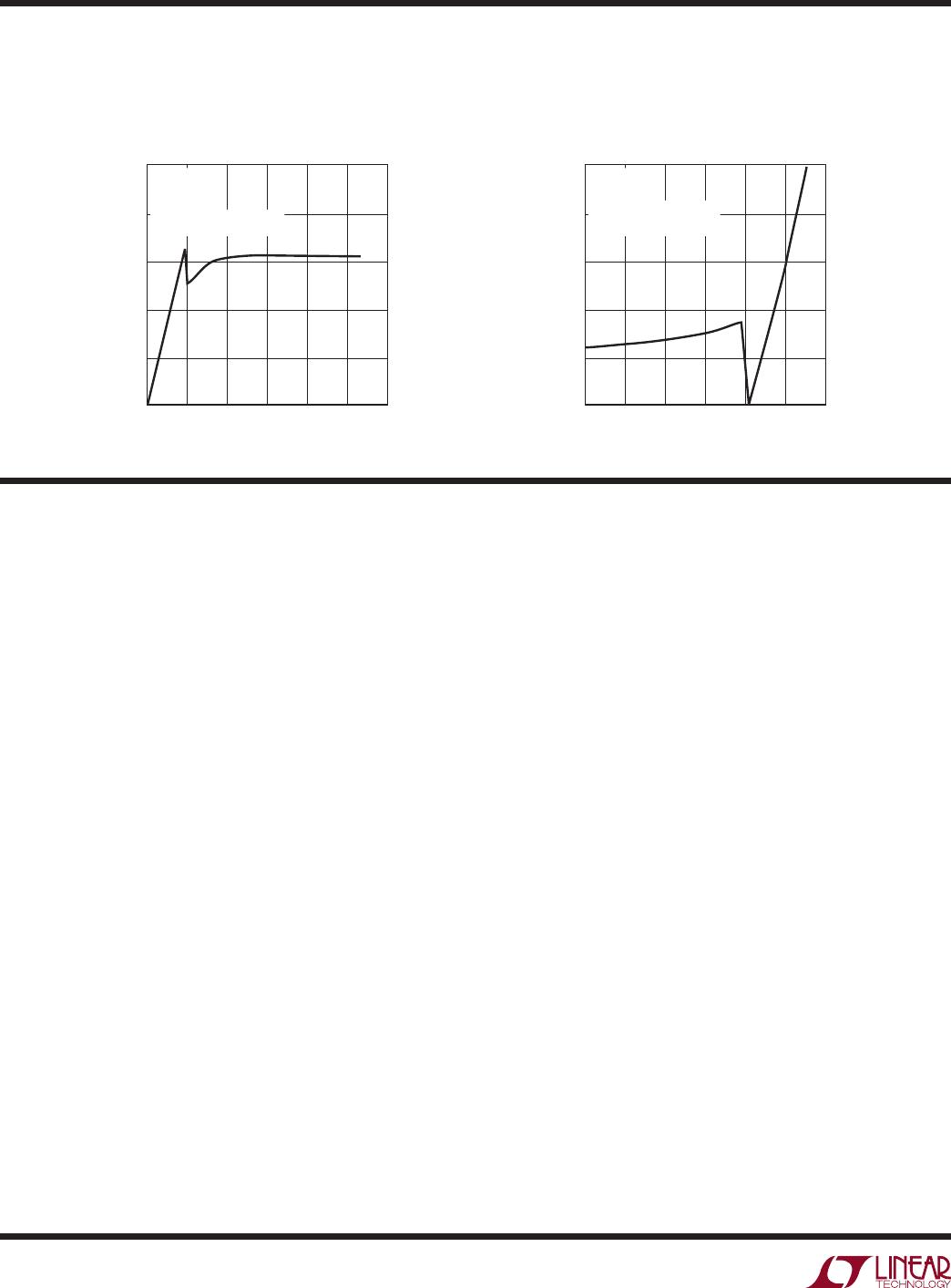
Short-Circuit Output Current vs
V
OUT
(Sinking)
Short-Circuit Output Current vs
V
OUT
(Sourcing)
1V/DIV
0
0
10mA/DIV
10
20
30
40
50
1
2 3 4
2607 G32
5 6
V
CC
= 5.5V
V
REF
= 5.6V
CODE = 0
V
OUT
SWEPT 0V TO V
CC
1V/DIV
0
–50
10mA/DIV
–40
–30
–20
–10
0
1
2 3 4
2607 G33
5 6
V
CC
= 5.5V
V
REF
= 5.6V
CODE = FULL SCALE
V
OUT
SWEPT V
CC
TO 0V
LTC2607/LTC2617/LTC2627
typical perFormance characteristics