Document Number: 93581 For technical questions within your region, please contact one of the following: www.vishay.com
Revision: 02-Jul-10 DiodesAmericas@vishay.com
, DiodesAsia@vishay.com, DiodesEurope@vishay.com 7
VSK.250, VSK.270, VSK.320 Series
Standard Recovery Diodes, 250 A to 320 A
(MAGN-A-PAK Power Modules)
Vishay Semiconductors
Fig. 16 - Forward Power Loss Characteristics
Fig. 17 - Forward Power Loss Characteristics
Fig. 18 - Forward Power Loss Characteristics
0 25 50 75 100 125 150
0
.
2
5
K
/
W
0
.
3
K
/
W
0
.
1
K
/
W
0
.
1
6
K
/
W
0
.
4
K
/
W
Maximum Allowable Ambient Temperature (°C)
0
.
0
6
K
/
W
R
=
0
.
0
2
K
/
W
-
D
e
l
t
a
R
t
h
S
A
0
.
6
K
/
W
0
100
200
300
400
500
600
700
0 50 100 150 200 250 300 350 400
DC
180°
(Sine)
Maximum Total Forward Power Loss (W)
To t a l RM S O u t p u t C u r r e n t ( A )
VSK.270.. Serie s
Pe r Ju n c t io n
T = 1 5 0 ° C
J
0 255075100125150
0
.
3
K
/
W
0
.
2
5
K
/
W
0
.
4
K
/
W
0
.
0
6
K
/
W
0
.
0
8
K
/
W
0
.
1
2
K
/
W
0
.
1
6
K
/
W
Maximum Allowable Ambient Temperature (°C)
0
.
0
4
K
/
W
R
=
0
.
0
2
K
/
W
-
D
e
l
t
a
R
0
.
6
K
/
W
t
h
S
A
0
200
400
600
800
1000
1200
1400
1600
1800
0 100 200 300 400 500 600
180°
(Sine)
180°
(Rec t)
Maximum Total Power Loss (W)
Total Output Current (A)
2 x VSK.270.. Se rie s
Single Phase Bridg e
Connected
T = 1 5 0 ° C
J
0 255075100125150
0
.
0
6
K
/
W
0
.
1
K
/
W
0
.
1
6
K
/
W
0
.
2
5
K
/
W
0
.
4
K
/
W
0
.
6
K
/
W
Maximum Allowable Ambient Temperature (°C)
R
=
0
.
0
2
K
/
W
-
D
e
l
t
a
R
0
.
0
4
K
/
W
t
h
S
A
0
300
600
900
1200
1500
1800
2100
2400
0200400600800
120°
(Rect)
Maximum Total Power Loss (W)
Total Output Current (A)
3 x VSK.270.. Se ries
Three Phase Bridge
Connected
T = 150°C
J
www.vishay.com For technical questions within your region, please contact one of the following: Document Number: 93581
8 DiodesAmericas@vishay.com
, DiodesAsia@vishay.com, DiodesEurope@vishay.com Revision: 02-Jul-10
VSK.250, VSK.270, VSK.320 Series
Vishay Semiconductors
Standard Recovery Diodes, 250 A to 320 A
(MAGN-A-PAK Power Modules)
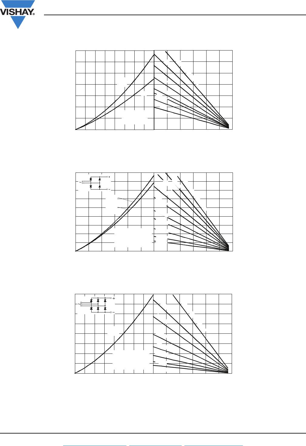
Fig. 19 - Maximum Non-Repetitive Surge Current
Fig. 20 - Maximum Non-Repetitive Surge Current
Fig. 21 - Forward Voltage Drop Characteristics
Fig. 22 - Thermal Impedance Z
thJC
Characteristics
Fig. 23 - Current Ratings Characteristics
Fig. 24 - Current Ratings Characteristics
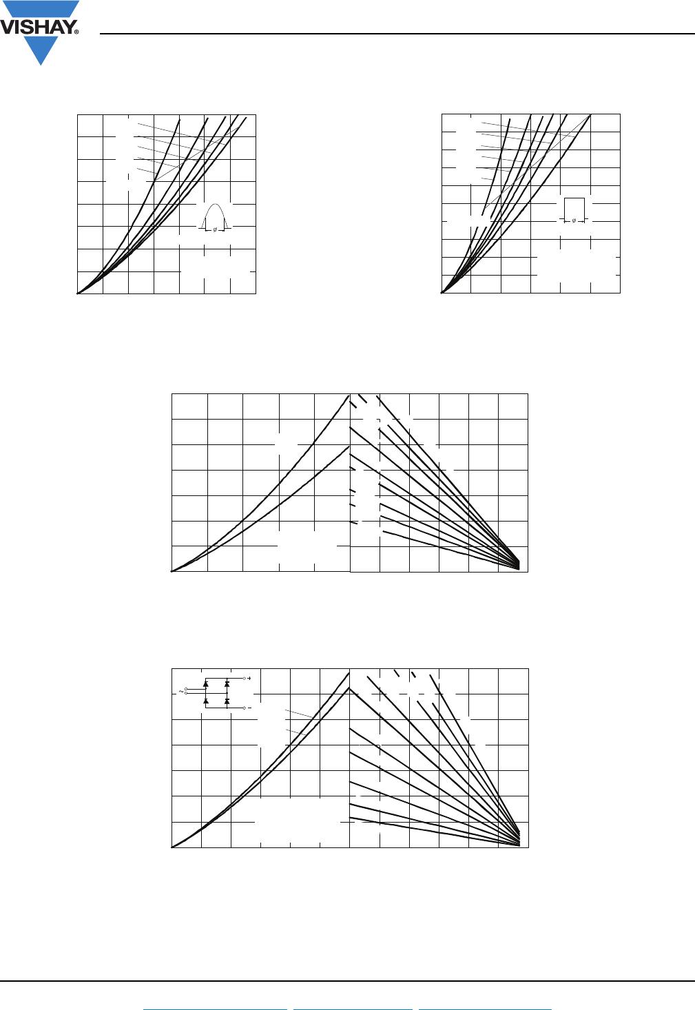
2000
3000
4000
5000
6000
7000
8000
110100
Pea k Ha lf Sine Wave Forward Current (A)
Number Of Equal Amplitude Half Cycle Current Pulses (N)
Initial T = 150°C
@ 60 Hz 0.0083 s
@ 50 Hz 0.0100 s
At Any Rated Load Condition And With
Rated V Applied Following Surge.
RRM
J
VSK.270.. Se rie s
Pe r Ju n c t io n
2000
3000
4000
5000
6000
7000
8000
9000
0.01 0.1 1
Pe a k Ha lf Sine Wave Forward Current (A)
Pu lse Tra i n D u ra t io n ( s)
Ma ximum Non Repetitive Surge Current
VSK.270.. Series
Pe r Ju n c t io n
Initia l T = 150°C
No Volta ge Rea p p lied
Ra t e d V Re a p p l ie d
Versus Pulse Train Duration.
RRM
J
10
100
1000
10000
0.511.522.533.54
T = 2 5 ° C
J
Instantaneous Forward Current (A)
Instantaneous Forward Voltage (V)
T = 150°C
J
VSK.270.. Se ries
Pe r Ju n c t io n
0.001
0.01
0.1
1
0.001 0.01 0.1 1 10 100
Sq ua re Wave Pulse Dura tio n (s)
thJC
Steady State Value:
R = 0.45 K/ W
(DC Operation)
thJC
VSK.270.. Serie s
Pe r Ju n c t io n
Transient Thermal Impeda nce Z (K/ W)
80
90
100
110
120
130
140
150
0 50 100 150 200 250 300 350
30°
60°
90°
120°
180°
Maximum Allowable Case Temperature (°C)
Conduction Angle
Average Forward Current (A)
VSK.320.. Se rie s
R ( D C ) = 0 . 12 5 K/ W
thJC
80
90
100
110
120
130
140
150
0 100 200 300 400 500 600
DC
30°
60°
90°
120°
180°
Maximum Allowable Case Temperature (°C)
Conduction Period
Averag e Forw a rd Current (A)
VSK.320.. Se ries
R ( DC ) = 0 . 12 5 K/ W
thJC
Document Number: 93581 For technical questions within your region, please contact one of the following: www.vishay.com
Revision: 02-Jul-10 DiodesAmericas@vishay.com
, DiodesAsia@vishay.com, DiodesEurope@vishay.com 9
VSK.250, VSK.270, VSK.320 Series
Standard Recovery Diodes, 250 A to 320 A
(MAGN-A-PAK Power Modules)
Vishay Semiconductors
Fig. 25 - Forward Power Loss Characteristics Fig. 26 - Forward Power Loss Characteristics
Fig. 27 - Forward Power Loss Characteristics
Fig. 28 - Forward Power Loss Characteristics
0
50
100
150
200
250
300
350
400
0 50 100 150 200 250 300 350
Average Forward Current (A)
RM S Li m i t
Maximum Average Forward Power Loss (W)
Conduction Angle
180°
120°
90°
60°
30°
VSK.320.. Se ries
T = 150°C
J
0
50
100
150
200
250
300
350
400
450
500
0 100 200 300 400 500 600
DC
180°
120°
90°
60°
30°
RMS Li m it
Conduc tion Period
Average Forward Current (A)
Maximum Average Forward Power Loss (W)
VSK.320.. Serie s
Pe r Ju n c t i o n
T = 150°C
J
0 25 50 75 100 125 150
0
.
1
K
/
W
0
.
2
K
/
W
0
.
6
K
/
W
0
.
0
6
K
/
W
0
.
3
K
/
W
0
.
4
K
/
W
Maximum Allowable Ambient Temperature (°C)
R
=
0
.
0
2
K
/
W
-
D
e
l
t
a
R
0
.
1
6
K
/
W
0
.
0
4
K
/
W
t
h
S
A
0
100
200
300
400
500
600
700
0 100 200 300 400 500
DC
180°
(Sine)
Total RMS Output Current (A)
VSK.320.. Serie s
Pe r Ju nc t io n
T = 150°C
Maximum Total Forward Power Loss (W)
J
0255075100125150
0
.
6
K
/
W
0
.
0
4
K
/
W
0
.
0
6
K
/
W
0
.
1
2
K
/
W
0
.
2
5
K
/
W
0
.
5
K
/
W
Maximum Allowable Ambient Temperature (°C)
R
=
0
.
0
2
K
/
W
-
D
e
l
t
a
R
0
.
1
6
K
/
W
t
h
S
A
0
.
0
8
K
/
W
0
.
0
3
K
/
W
0
200
400
600
800
1000
1200
1400
0 100 200 300 400 500 600
180°
(Sine)
180°
(Rec t)
M a xi m u m To t a l Po w e r Lo ss ( W)
Total Output Current (A)
2 x VSK.320.. Series
Si n g l e Ph a se Br i d g e
Connec ted
T = 150°C
J

VSKD250-16

Mfr. #:
Manufacturer:
Vishay
Description:
DIODE MODULE 1.6KV 250A MAGNAPAK
Lifecycle:
New from this manufacturer.
Delivery:
DHL FedEx Ups TNT EMS
Payment:
T/T Paypal Visa MoneyGram Western Union