www.vishay.com For technical questions within your region, please contact one of the following: Document Number: 93581
10 DiodesAmericas@vishay.com
, DiodesAsia@vishay.com, DiodesEurope@vishay.com Revision: 02-Jul-10
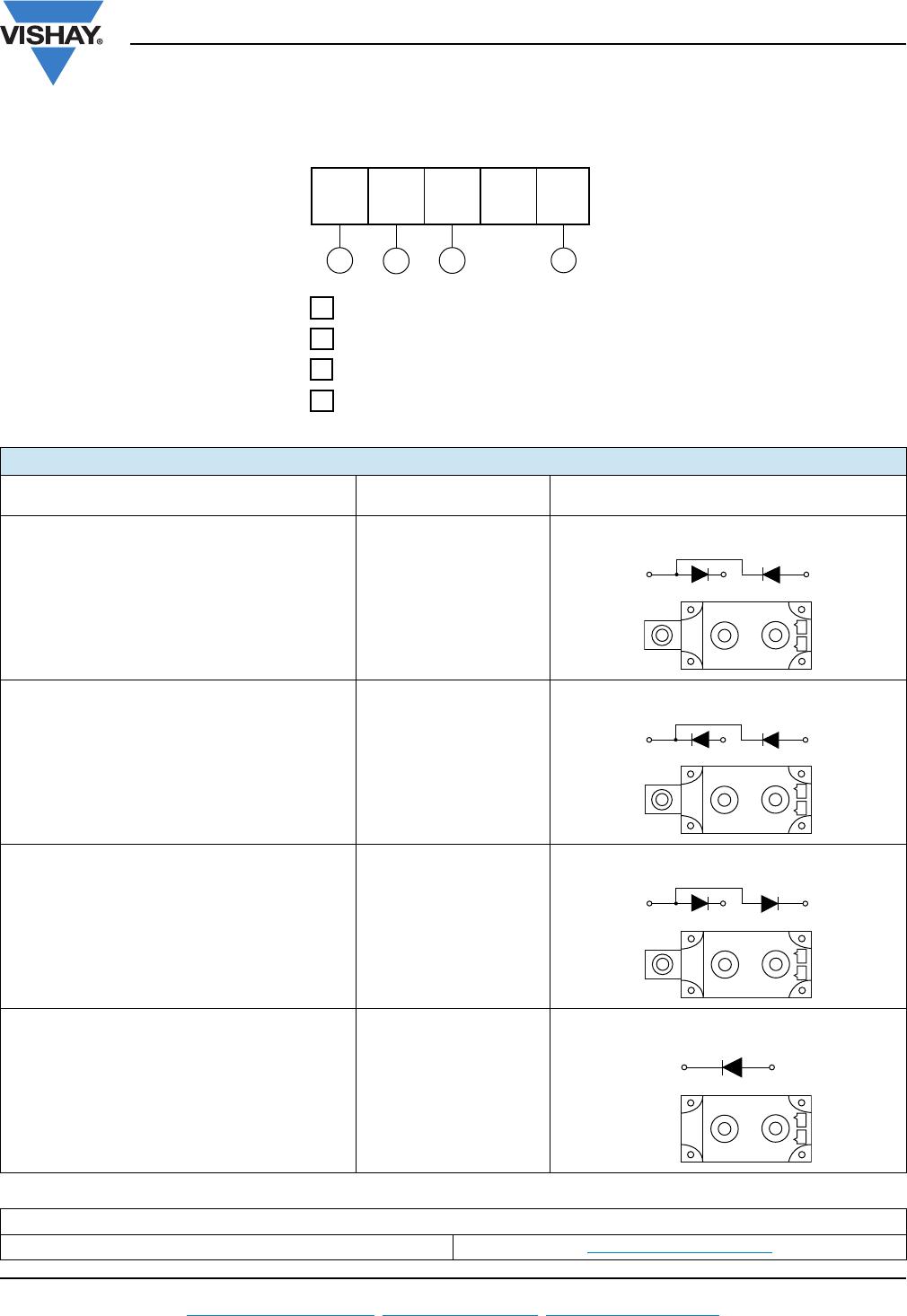
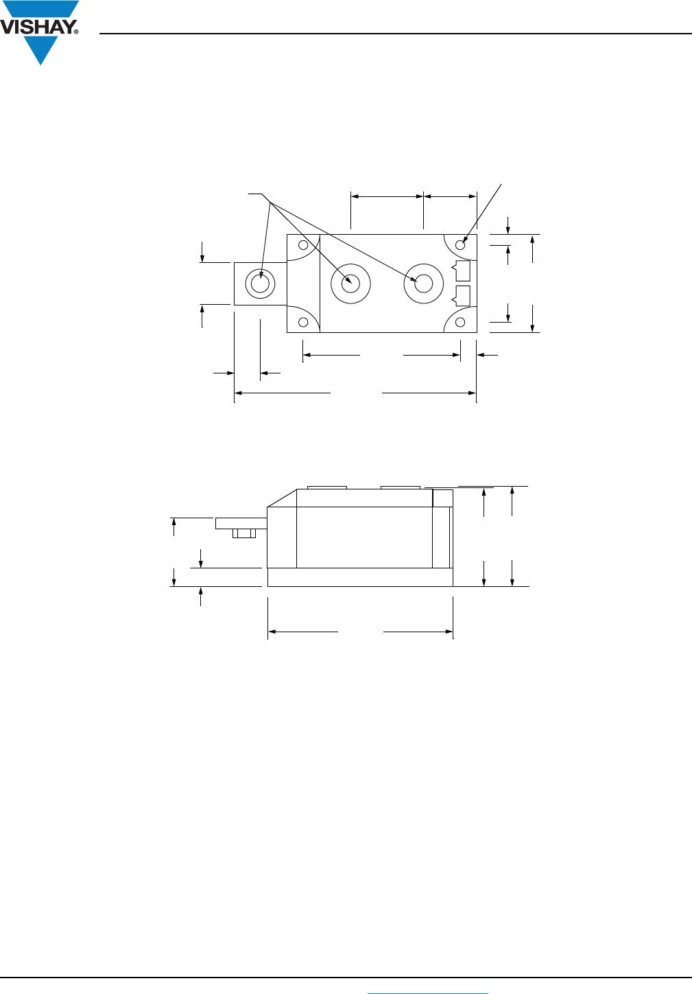
VSK.250, VSK.270, VSK.320 Series
Vishay Semiconductors
Standard Recovery Diodes, 250 A to 320 A
(MAGN-A-PAK Power Modules)
Fig. 29 - Forward Power Loss Characteristics
Fig. 30 - Maximum Non-Repetitive Surge Current
Fig. 31 - Maximum Non-Repetitive Surge Current
Fig. 32 - Forward Voltage Drop Characteristics
Fig. 33 - Thermal Impedance Z
thJC
Characteristics
0 25 50 75 100 125 150
0
.
0
4
K
/
W
0
.
0
5
K
/
W
0
.
0
6
K
/
W
0
.
1
2
K
/
W
0
.
3
K
/
W
0
.
6
K
/
W
Maximum Allowable Ambient Temperature (°C)
0.
0
3
K
/W
R
=
0
.
0
2
K
/
W
-
D
e
l
t
a
R
0
.
2
K
/
W
0
.
0
8
K
/
W
t
h
S
A
0
400
800
1200
1600
2000
2400
2800
0 200 400 600 800 1000
120°
(Rect)
Total Output Current (A)
M a x im u m To t a l Po w e r Lo ss ( W )
3 x VSK.320.. Series
Three Phase Bridge
Connected
T = 15 0 ° C
J
2000
3000
4000
5000
6000
7000
8000
9000
10000
110100
Peak Half Sine Wave Forward Current (A)
Number Of Equal Amplitude Half Cycle Current Pulses (N)
VSK.320.. Series
Pe r Ju n c t io n
Initial T = 150°C
@ 60 Hz 0.0083 s
@ 50 Hz 0.0100 s
At Any Rated Load Condition And With
Rated V App lied Fo llowing Surge.
RRM
J
2000
3000
4000
5000
6000
7000
8000
9000
10000
0.01 0.1 1
Peak Half Sine Wave Forward Current (A)
Pulse Train Duration (s)
Maximum Non Repetitive Surge Current
Initia l T = 150°C
No Voltage Reapplied
Ra t e d V Re a p p l i e d
Versus Pulse Train Duration.
RRM
J
VSK.320.. Series
Pe r Ju n c t io n
100
1000
10000
0.5 1 1.5 2 2.5 3 3.5 4
T = 2 5° C
J
Instantaneous Forward Current (A)
In st a n t a n e o u s Fo rw a rd V o lt a g e ( V)
VSK.320.. Se ries
Pe r Ju n c t io n
T = 1 5 0 ° C
J
0.001
0.01
0.1
1
0.001 0.01 0.1 1 10 100
Square Wave Pulse Duration (s)
thJC
Transient T
hermal Imp eda nc e Z (K/ W)
VSK.320.. Series
Pe r Ju n c t io n
St e a d y St a t e V a l u e :
R = 0. 45 K/ W
(DC Operation)
thJC