NL17SG14P5T5G

NL17SG14
www.onsemi.com
4
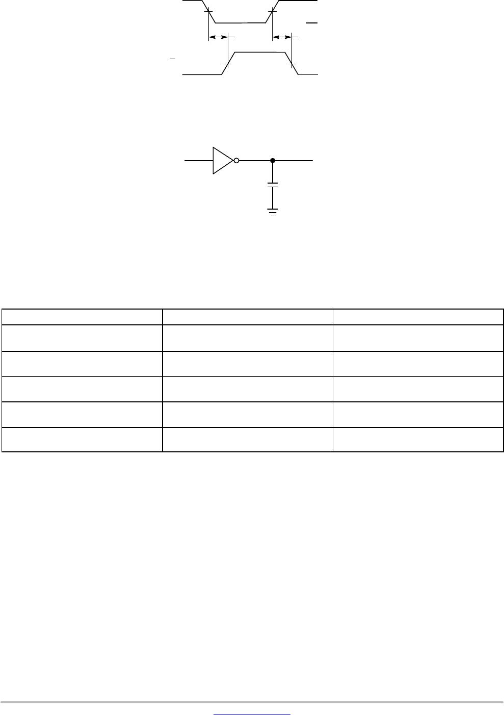
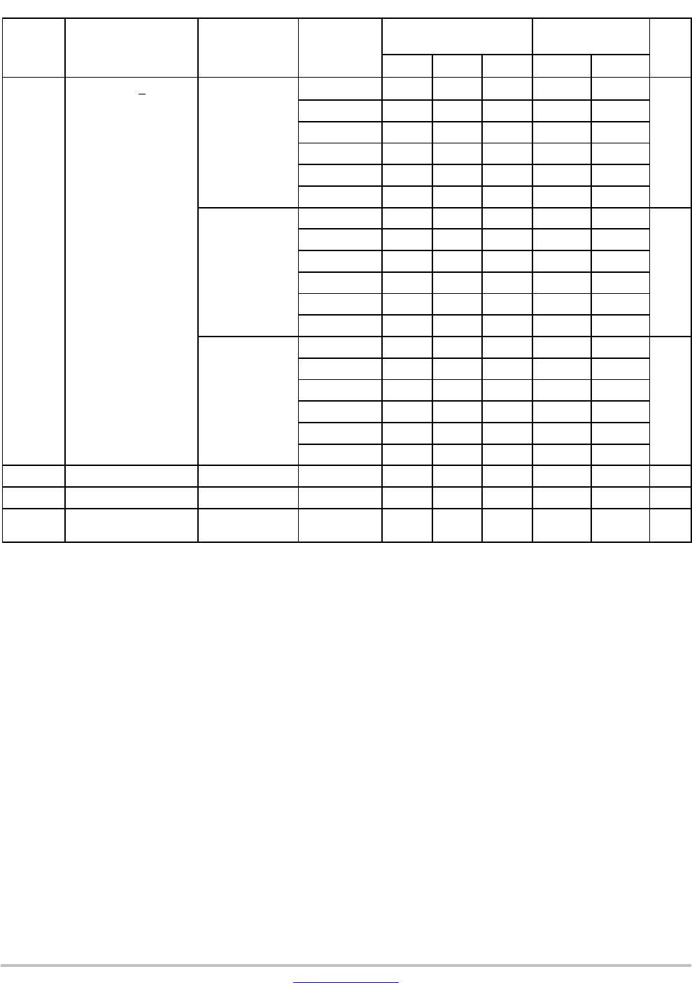
AC ELECTRICAL CHARACTERISTICS (Input t
r
= t
f
= 3.0 ns)
Symbol Parameter Test Condition V
CC
(V)
T
A
= 25 5C
T
A
=
−555C to +1255C
Unit
Min Typ Max Min Max
t
PLH
,
t
PHL
Propagation Delay,
A or Y
C
L
= 10 pF,
R
L
= 1 MW
0.9 27.3
ns
1.1 to 1.3 13.0 22.6 1.0 35.9
1.4 to 1.6 7.5 10.5 1.0 11.3
1.65 to 1.95 6.0 7.8 1.0 8.2
2.3 to 2.7 4.3 5.4 1.0 5.8
3.0 to 3.6 3.5 4.4 1.0 4.6
C
L
= 15 pF,
R
L
= 1 MW
0.9 29.5
ns
1.1 to 1.3 14.3 25.1 1.0 41.6
1.4 to 1.6 8.0 11.5 1.0 12.6
1.65 to 1.95 6.3 8.4 1.0 8.7
2.3 to 2.7 4.6 5.7 1.0 6.1
3.0 to 3.6 3.7 4.6 1.0 5.0
C
L
= 30 pF,
R
L
= 1 MW
0.9 40.5
ns
1.1 to 1.3 19.6 35.7 1.0 58.1
1.4 to 1.6 10.7 15.8 1.0 17.6
1.65 to 1.95 7.8 10.7 1.0 11.7
2.3 to 2.7 5.4 6.9 1.0 8.1
3.0 to 3.6 4.3 5.2 1.0 6.1
C
IN
Input Capacitance 0 to 3.6 3 pF
C
O
Output Capacitance V
O
= GND 0 3 pF
C
PD
Power Dissipation
Capacitance (Note 5)
f = 10 MHz 0.9 to 3.6 4 pF
Product parametric performance is indicated in the Electrical Characteristics for the listed test conditions, unless otherwise noted. Product
performance may not be indicated by the Electrical Characteristics if operated under different conditions.
5. C
PD
is defined as the value of the internal equivalent capacitance which is calculated from the dynamic operating current consumption without
load. Average operating current can be obtained by the equation: I
CC(OPR
)
= C
PD
V
CC
f
in
+ I
CC
. C
PD
is used to determine the no−load
dynamic power consumption; P
D
= C
PD
V
CC
2
f
in
+ I
CC
V
CC
.
NL17SG14
www.onsemi.com
5
Figure 5. Switching Waveform
Figure 6. Test Circuit
V
CC
GND
50%
50% V
CC
A or B
Y
t
PHL
t
PLH
INPUT
C
L
*
*Includes all probe and jig capacitance.
A 1 MHz square input wave is recommended for
propagation delay tests.
OUTPUT
ORDERING INFORMATION
Device Package Shipping
NL17SG14P5T5G SOT−953
(Pb−Free)
8000 / Tape & Reel
NL17SG14DFT2G SC−88A
(Pb−Free)
3000 / Tape & Reel
NLV17SG14DFT2G* SC−88A
(Pb−Free)
3000 / Tape & Reel
NL17SG14AMUTCG
(In Development)
UDFN6 1.45x1 mm
(Pb−Free)
3000 / Tape & Reel
NL17SG14CMUTCG
(In Development)
UDFN6 1x1 mm
(Pb−Free)
3000 / Tape & Reel
For information on tape and reel specifications, including part orientation and tape sizes, please refer to our Tape and Reel Packaging
Specifications Brochure, BRD8011/D.
*NLV Prefix for Automotive and Other Applications Requiring Unique Site and Control Change Requirements; AEC−Q100 Qualified and PPAP
Capable.
NL17SG14
www.onsemi.com
6
PACKAGE DIMENSIONS
SOT−953
CASE 527AE
ISSUE E
*For additional information on our Pb−Free strategy and soldering
details, please download the ON Semiconductor Soldering and
Mounting Techniques Reference Manual, SOLDERRM/D.
SOLDERING FOOTPRINT*
E
D
C
A
H
E
123
45
NOTES:
1. DIMENSIONING AND TOLERANCING PER ASME
Y14.5M, 1994.
2. CONTROLLING DIMENSION: MILLIMETERS
3. MAXIMUM LEAD THICKNESS INCLUDES LEAD
FINISH. MINIMUM LEAD THICKNESS IS THE
MINIMUM THICKNESS OF THE BASE MATERIAL.
4. DIMENSIONS D AND E DO NOT INCLUDE MOLD
FLASH, PROTRUSIONS, OR GATE BURRS.
DIM MIN NOM MAX
MILLIMETERS
A 0.34 0.37 0.40
b 0.10 0.15 0.20
C 0.07 0.12 0.17
D 0.95 1.00 1.05
E 0.75 0.80 0.85
e 0.35 BSC
L
0.95 1.00 1.05
H
E
X
Y
PIN ONE
INDICATOR
b
5X
X0.08 Y
L
5X
L3
L2
e
5X
5X
L2 0.05 0.10 0.15
L3 −− −−− 0.15
0.175 REF
TOP VIEW
SIDE VIEW
BOTTOM VIEW
1.20
DIMENSIONS: MILLIMETERS
0.20
5X
1
PACKAGE
OUTLINE
0.35
PITCH
0.35
5X

NL17SG14P5T5G

Mfr. #:
Manufacturer:
ON Semiconductor
Description:
Inverters SCHMITT INVERTER
Lifecycle:
New from this manufacturer.
Delivery:
DHL FedEx Ups TNT EMS
Payment:
T/T Paypal Visa MoneyGram Western Union

Products related to this Datasheet