AX−SFUS, AX−SFUS−API
www.onsemi.com
4
Table 1. PIN FUNCTION DESCRIPTIONS
DescriptionTypePin(s)Symbol
CLKP 40 A TCXO interface
GND Center pad P Ground on center pad of QFN, must be connected
A = analog input
I = digital input signal
O = digital output signal
PU = pull−up
I/O = digital input/output signal
N = not to be connected
P = power or ground
PD = pull−down
All digital inputs are Schmitt trigger inputs, digital input
and output levels are LVCMOS/LVTTL compatible. Pins
GPIO[3:0] must not be driven above VDD_IO, all other
digital inputs are 5 V tolerant. All GPIO pins and UARTRX
start up as input with pull−up. For explanations on how to
use the GPIO pins, see chapter “AT Commands”.
Table 2.
Pin Possible GPIO Modes
GPIO0 0, 1, Z, U, A, T
GPIO1 0, 1, Z, U, A
GPIO4 0, 1, Z, U, T
GPIO5 0, 1, Z, U
GPIO6 0, 1, Z, U
GPIO7 0, 1, Z, U
GPIO8 0, 1, Z, U
GPIO9 0, 1, Z, U
0 = pin drives
1 = not to be connected
Z = pin is high impedance input
U = pin is input with pull−up
A = pin is analog input
T = pin is driven by clock or DAC
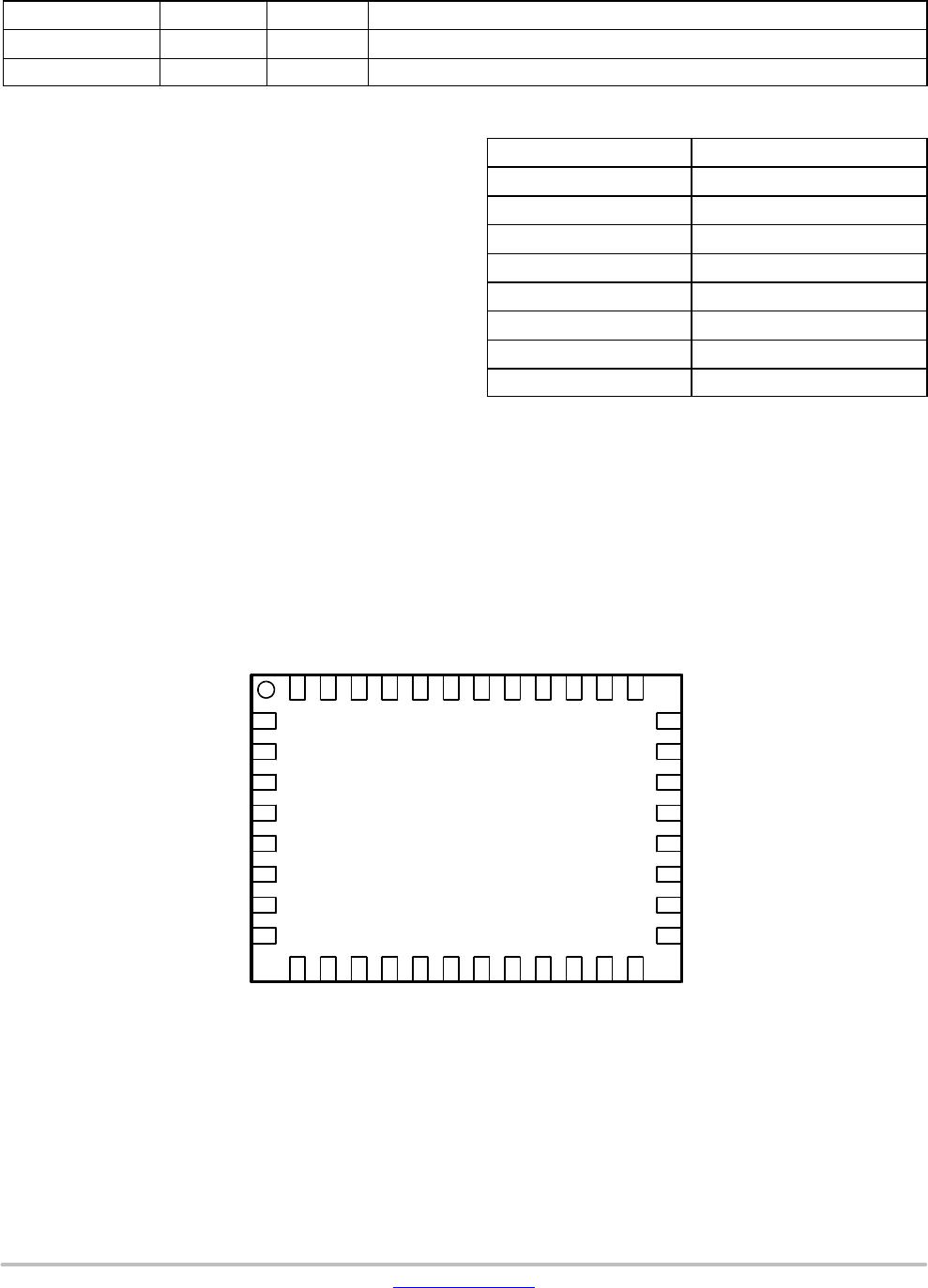
Pinout Drawing
Figure 2. Pinout Drawing (Top View)
AX−SFEU / AX−SFEU−API
QFN40
8
7
6
5
4
3
2
1
9 10 11 12 13 14 15 16 17 18 19 20
21
22
23
24
25
26
27
28
40 39 38 37 36 35 34 33 32 31 30 29
VDD_ANA
ANTP
GND
ANTN
ANTP1
GND
GND
VDD_ANA
FILT
CLKP
CLKN
NC
CAL
VDD_IO
NC
GPIO0
VDD_IO
GND
RESET_N
GPIO1
TX_EN
NC
RX_EN
L2
L1
NC
GPIO8
GPIO7
GPIO6
GPIO5
GPIO4
CPU_LED
RADIO_LED
VTCXO
GPIO9
UARTTX
UARTRX
RXLED
TXLED
NC
AX−SFUS, AX−SFUS−API
www.onsemi.com
5
SPECIFICATIONS
Table 3. ABSOLUTE MAXIMUM RATINGS
Symbol Description Condition Min Max Units
VDD_IO Supply voltage −0.5 5.5 V
IDD Supply current 200 mA
P
tot
Total power consumption 800 mW
P
i
Absolute maximum input power at receiver input ANTP and ANTN
pins in RX mode
10 dBm
I
I1
DC current into any pin except ANTP, ANTN, ANTP1 −10 10 mA
I
I2
DC current into pins ANTP, ANTN, ANTP1 −100 100 mA
I
O
Output Current 40 mA
V
ia
Input voltage ANTP, ANTN, ANTP1 pins −0.5 5.5 V
Input voltage digital pins −0.5 5.5 V
V
es
Electrostatic handling HBM −2000 2000 V
T
amb
Operating temperature −40 85 °C
T
stg
Storage temperature −65 150 °C
T
j
Junction Temperature 150 °C
Stresses exceeding those listed in the Maximum Ratings table may damage the device. If any of these limits are exceeded, device functionality
should not be assumed, damage may occur and reliability may be affected.
1. Exposure to absolute maximum rating conditions for extended periods may affect device reliability.
AX−SFUS, AX−SFUS−API
www.onsemi.com
6
DC Characteristics
Table 4. SUPPLIES
Conditions for all current and charge values unless otherwise specified are for the hardware configuration described in the AX−SFUS
Application Note: Sigfox Compliant Reference Design.
Symbol Description Condition Min Typ Max Units
T
AMB
Operational ambient temperature −40 27 85 °C
VDD
IO
I/O and voltage regulator supply
voltage AX−SFUS chip only
1.8* 3.0 3.6 V
VDD
IO_mod
I/O and voltage regulator supply
voltage AX−SFUS with RF frontend
module as in Figure 5
2.7 3.3 3.6 V
VDD
IO_R1
I/O voltage ramp for reset activation;
Note 1
Ramp starts at VDD_IO 0.1 V 0.1 V/ms
VDD
IO_R2
I/O voltage ramp for reset activation;
Note 1
Ramp starts at 0.1 V < VDD_IO < 0.7 V 3.3 V/ms
I
DS
Deep sleep mode current; Note 3 AT$P=2 350 nA
I
SLP
Sleep mode current; Note 3 AT$P=1 1.6
mA
I
STDBY
Standby mode current
Notes 2, 3
0.5 mA
I
RX_CONT
Current consumption continuous
RX; Note 3
AT$TM=3,255 34 mA
Q
SFX_OOB_24
Charge to send a Sigfox out of band
message, 24 dBm; Note 3
AT$S0 0.25 C
Q
SFX_BIT_24
Charge to send a bit, 24 dBm;
Note 3
AT$SB=0 0.22 C
Q
SFX_BITDL_24
Charge to send a bit with downlink
receive, 24 dBm; Note 3
AT$SB=0,1 0.28 C
Q
SFX_LFR_24
Charge to send the longest possible
Sigfox frame (12 byte) , 24 dBm;
Note 3
AT$SF=00112233445566778899aabb 0.73 C
Q
SFX_LFRDL_24
Charge to send the longest possible
Sigfox frame (12 byte) with downlink
receive, 24 dBm; Note 3
AT$SF=00112233445566778899aabb,1 0.84 C
I
TXMOD24AVG
Modulated Transmitter Current;
Note 3
Pout=24 dBm; average 230 mA
*The device is operational from 1.8 V to 3.6 V. However, a supply voltage below 2.0 V is considered an extreme condition and operation can
lead to reduced output power and increased spurious emission.
1. If VDD_IO ramps cannot be guaranteed, an external reset circuit is recommended, see the AX8052 Application Note: Power On Reset
2. Internal 20 MHz oscillator, voltage conditioning and supervisory circuit running.
3. Includes Front End Module, TCXO.
AX-SFUS-API-1-01-TX30

Mfr. #:
Manufacturer:
ON Semiconductor
Description:
RF System on a Chip - SoC RF-MICROCONTROLLER
Lifecycle:
New from this manufacturer.
Delivery:
DHL FedEx Ups TNT EMS
Payment:
T/T Paypal Visa MoneyGram Western Union