DT1042-04SO-7

DT1042-04SO
Document number: DS36292 Rev. 2 - 2
1 of 5
www.diodes.com
September 2013
© Diodes Incorporated
DT1042-04SO
ADVANCE INFORMATION
4 CHANNEL LOW CAPACITANCE TVS DIODE ARRAY
Features
Low Clamping Voltage, I/O to V
SS
Typical 9V at 10A 100ns, TLP
Typical 7.7V at 6A 8μs/20μs
IEC 61000-4-2 (ESD): Air – +27/-19kV, Contact – ±16kV
IEC 61000-4-4 (EFT): Level-4
IEC 61000-4-5 (Lightning): ±6A
4 Channels of ESD protection
Low Channel Input Capacitance of 0.65pF Typical
TLP Dynamic Resistance: 0.25
Typically Used for High Speed Ports such as USB 2.0,
IEEE1394, HDMI, Laptop and Personal Computers, Flat Panel
Displays, Video Graphics Displays, SIM Ports
Totally Lead-Free & Fully RoHS Compliant (Notes 1 & 2)
Halogen and Antimony Free. “Green” Device (Note 3)
Mechanical Data
Case: SOT26
Case Material: Molded Plastic, “Green” Molding Compound.
UL Flammability Classification Rating 94V-0
Moisture Sensitivity: Level 1 per J-STD-020
Terminals: Matte Tin Finish annealed over Copper leadframe
(Lead Free Plating). Solderable per MIL-STD-202, Method 208
Weight: 0.016 grams (approximate)
Ordering Information
(Note 4)
Product Compliance Marking Reel Size (inches) Tape Width (mm) Quantity per Reel
DT1042-04SO-7 Standard BC1 7 8 3,000/Tape & Reel
Notes: 1. No purposely added lead. Fully EU Directive 2002/95/EC (RoHS) & 2011/65/EU (RoHS 2) compliant.
2. See http://www.diodes.com/quality/lead_free.html for more information about Diodes Incorporated’s definitions of Halogen- and Antimony-free, "Green"
and Lead-free.
3. Halogen- and Antimony-free "Green” products are defined as those which contain <900ppm bromine, <900ppm chlorine (<1500ppm total Br + Cl) and
<1000ppm antimony compounds.
4. For packaging details, go to our website at http://www.diodes.com/products/packages.html.
Marking Information
Date Code Key
Year 2013 2014 2015 2016 2017 2018
Code A B C D E F
Month Jan Feb Mar Apr May Jun Jul Aug Sep Oct Nov Dec
Code 1 2 3 4 5 6 7 8 9 O N D
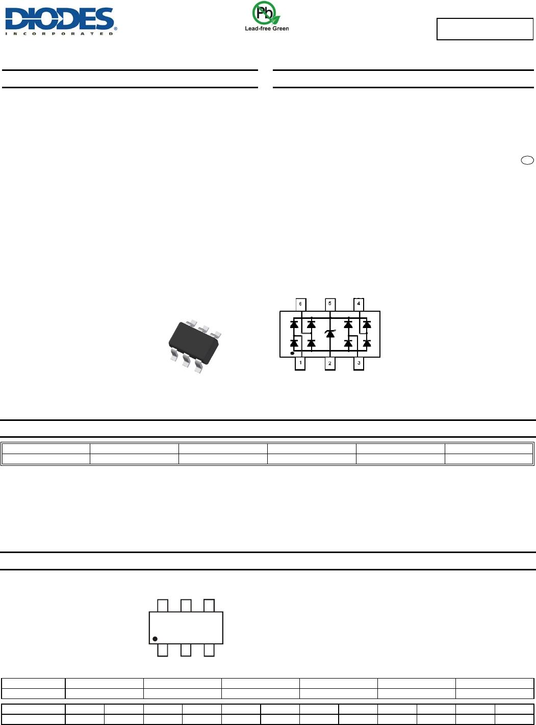
Top View
Device Schematic
BC1 = Product Type Marking Code
YM = Date Code Marking
Y = Year (ex: A = 2013)
M = Month (ex: 9 = September)
SOT26
A17
YM
BC1
I/O4
Vcc
Vss
I/O3
I/O2 I/O1
e3
DT1042-04SO
Document number: DS36292 Rev. 2 - 2
2 of 5
www.diodes.com
September 2013
© Diodes Incorporated
DT1042-04SO
ADVANCE INFORMATION
Maximum Ratings (@T
A
= +25°C, unless otherwise specified.)
Characteristic Symbol Value Unit Conditions
Peak Pulse Current, per IEC 61000-4-5
I
PP_I/O
±6 A
I/O to V
SS
, 8/20 μs
Peak Pulse Power, per IEC 61000-4-5
P
PP_I/O
55 W
I/O to V
SS
, 8/20 μs
Operating Voltage (DC)
V
DC
5.5 V
I/O to V
SS
ESD Protection – Contact Discharge, per IEC 61000-4-2
V
ESD_I/O
±16 kV
I/O to V
SS
ESD Protection – Air Discharge, per IEC 61000-4-2
V
ESD_I/O
+27/-19 kV
I/O to V
SS
Operating Temperature
T
OP
-55 to +85 °C
Storage Temperature
T
STG
-55 to +150 °C
Thermal Characteristics
Characteristic Symbol Value Unit
Power Dissipation Typical (Note 5)
P
D
300 mW
Thermal Resistance, Junction to Ambient Typical (Note 5)
R
θJA
417 °C/W
Electrical Characteristics (@T
A
= +25°C, unless otherwise specified.)
Characteristic Symbol Min Typ Max Unit Test Conditions
Reverse Working Voltage
VRWM
5.0 V
V
CC
to V
SS
Reverse Current (Note 6)
I
R(Vcc to Vss)
1.0 μA
V
R
= V
RWM
= 5V, V
CC
to V
SS
Reverse Current (Note 6)
I
R(IO to Vss)
0.5 μA
V
R
= V
RWM
= 5V, any I/O to V
SS
Reverse Breakdown Voltage
VBR
6.2
V
I
R
= 1mA, V
CC
to V
SS
Forward Clamping Voltage
V
F
-1.0 -0.8
V
I
F
= -15mA, V
CC
to V
SS
Reverse Clamping Voltage(Note 7)
V
C_Vcc
6.3
V
I
PP
= 9A, V
CC
to V
SS
, 8/20 μs
V
C_I/O
7.7 9 V
I
PP
= 6A, I/O to V
SS
, 8/20 μs
ESD Clamping Voltage
V
ESD_Vcc
6.8
V
TLP, 10A, tp = 100 ns, V
CC
to V
SS
,
per Fig. 8
V
ESD
_
I/O
9
V
TLP, 10A, tp = 100 ns, I/O to V
SS
,
per Fig. 8
Dynamic Resistance
R
DIF_Vcc
0.1
TLP, 10A, tp = 100 ns, V
CC
to V
SS
R
DIF_I/O
0.25
TLP, 10A, tp = 100 ns, I/O to V
SS
Channel Input Capacitance
C
I/O to
V
SS
0.65 0.8 pF
V
R
= 2.5V, V
CC
= 5V, f = 1MHz
Variation of Channel Input Capacitance
C
I/O
0.02
pF
V
CC
= 5V, V
SS
= 0V, I/O = 2.5V, f =1MHz,
T=+25°C , I/O_x to V
SS
– I/O_y to V
SS
Notes: 5. Device mounted on Polymide PCB pad layout (2oz copper) as shown on Diodes Inc. suggested pad layout AP02001, which can be found on our website
at http://www.diodes.com.
6. Short duration pulse test used to minimize self-heating effect.
7. Clamping voltage value is based on an 8x20µs peak pulse current (I
pp
) waveform.
DT1042-04SO
Document number: DS36292 Rev. 2 - 2
3 of 5
www.diodes.com
September 2013
© Diodes Incorporated
DT1042-04SO
ADVANCE INFORMATION
100
0 25 50 75 100 125 150 175 200
T , AMBIENT TEMPERATURE(°C)
A
Figure 1 Pulse Derating Curve
P
EAK
P
U
SLE DE
R
A
T
I
N
G
I
N
%
O
F
PEAK POWER OR CURRENT
75
25
0
50
6.0
6.5
7.0
7.5
8.0
8.5
9.0
9.5
-60
B
R
EAK
D
O
W
N
V
O
L
T
A
G
E,
T
R
I
G
G
E
R
V
O
L
T
A
G
E,
HOLDING VOLTAGE (V)
-40 -20 0 20 40 60 80 100 120 140 160
T , AMBIENT TEMPERATURE(°C)
A
Figure 2 Breakdown Voltage, Trigger Voltage,
Holding Voltage vs. Ambient Temperature
BV
VTRIG
VH
5.0
5.5
6.0
6.5
7.0
7.5
8.0
012345678910
,
IEC61000-4-5 (Lighting)
CURRENT FROM I/O TO V (A)
Figure 3 Clamping Voltage Characteristics
SS
CURRENT FROM V TO V (A)
CC SS
V,
C
LAM
P
IN
G
V
O
L
T
A
G
E (V)
C
V to V
CC SS
I/O to V
SS
0.0
0.5
1.0
1.5
2.0
2.5
3.0
012345678910
V,
F
O
WA
R
D V
O
L
T
A
G
E (V)
F
CURRENT FROM TO (A)
Figure 4 Forward Voltage Characteristics
VI/O
CURRENT FROM V TO V (A)
SS
SS CC
IEC61000-4-5
(Lighting)
V to V
SS CC
V to I/O
SS
0
1
2
3
4
5
6
7
8
9
10
TIME (µs)
Figure 5 Waveform of Clamping Voltage,
Current vs. Time (8/20 s, I/O to V )µ
SS
C
LA
M
P
I
N
G
V
O
L
T
A
G
E,
C
U
R
R
E
N
T
(V, A)
-40 -30 -20 -10 0 10 20 30 40 50 60 70 80
Ampere
Voltage
0
1
2
3
4
5
6
7
8
9
10
-40-30-20-10 0 102030405060
TIME (µs)
Figure 6 Waveform of Clamping Voltage,
Current vs. Time (8/20 s, to V )µ
SS
V
CC
C
LAM
P
I
N
G
V
O
L
T
A
G
E,
C
U
R
R
E
N
T
(V, A)
Ampere
Voltage

DT1042-04SO-7

Mfr. #:
Manufacturer:
Diodes Incorporated
Description:
TVS Diodes / ESD Suppressors 4-Ch Low Cap TVS Array .65pF 6A 300mW
Lifecycle:
New from this manufacturer.
Delivery:
DHL FedEx Ups TNT EMS
Payment:
T/T Paypal Visa MoneyGram Western Union

Products related to this Datasheet