Expand menu
Hello, Sign in
My Account
0
Cart
Home
Products
Sensors
Semiconductors
Passive Components
Connectors
Power
Electromechanical
Optoelectronics
Circuit Protection
Integrated Circuits - ICs
Main Products
Manufacturers
Blog
Services
About OMO
About Us
Contact Us
Check Stock
PESD7V0C1BSFYL
P1-P3
P4-P6
P7-P9
P10-P12
Nexperia
PESD7V0C1BSF
Ultra low capacitance bidirectional ESD protection diode
PESD7V0C1BSF
All information provided in this document is subject to legal disclaimers.
©
Nexperia B.V. 2017. All rights reserved
Product data sheet
17 December 2017
4 / 12
9. Characteristics
Table 6. Characteristics
Symbol
Parameter
Conditions
Min
Typ
Max
Unit
V
RWM
reverse standoff
voltage
T
amb
= 25 °C
-
-
7
V
V
BR
breakdown voltage
I
R
= 1 mA; T
amb
= 25 °C
7.5
9
11
V
I
RM
reverse leakage
current
V
RWM
= 7 V; T
amb
= 25 °C
-
1
50
nA
f = 1 MHz; V
R
= 0 V; T
amb
= 25 °C
-
0.2
0.25
pF
C
d
diode capacitance
f = 2.5 GHz; V
R
= 0 V
-
0.2
-
pF
I
PPM
= 9 A; t
p
= 8/20 µs; T
amb
= 25 °C
[1]
-
-
5.5
V
I
PP
= 8 A; t
p
= TLP; T
amb
= 25 °C
[2]
-
4.6
-
V
V
CL
clamping voltage
I
PP
= 16 A; t
p
= TLP; T
amb
= 25 °C
[2]
-
6.5
-
V
R
dyn
dynamic resistance
I
R
= 10 A; T
amb
= 25 °C
[2]
-
0.23
-
Ω
[1]
According to IEC 61000-4-5 and IEC 61643-321.
[2]
Non-repetitive current pulse, Transmission Line Pulse (TLP) t
p
= 100 ns; square pulse; ANSI / ESD STM5.5.1-2008.
006aab325
-V
CL
-V
BR
-V
RWM
V
CL
V
BR
V
RWM
-I
RM
I
RM
-I
R
I
R
-I
PP
I
PP
-
+
I
PPM
-I
PPM
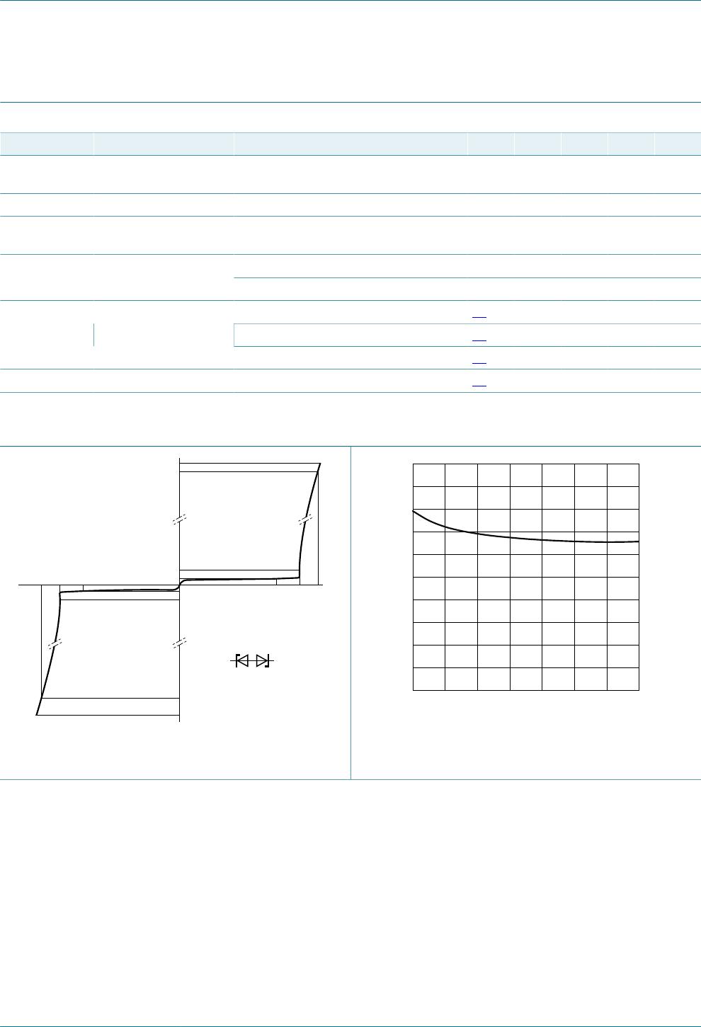
Fig. 3.
V-I characteristics for a bidirectional ESD
protection diode
V
R
(V)
7
5
1
6
4
2
0
3
aaa-027220
0.25
C
d
(pF)
0
0.05
0.10
0.15
0.20
f = 1 MHz; T
amb
= 25 °C
Fig. 4.
Diode capacitance as a function of reverse
voltage; typical values
Nexperia
PESD7V0C1BSF
Ultra low capacitance bidirectional ESD protection diode
PESD7V0C1BSF
All information provided in this document is subject to legal disclaimers.
©
Nexperia B.V. 2017. All rights reserved
Product data sheet
17 December 2017
5 / 12
f (GHz)
0
8
6
2
4
aaa-016862
0.10
0.15
0.05
0.20
0.25
C
d
(pF)
0.00
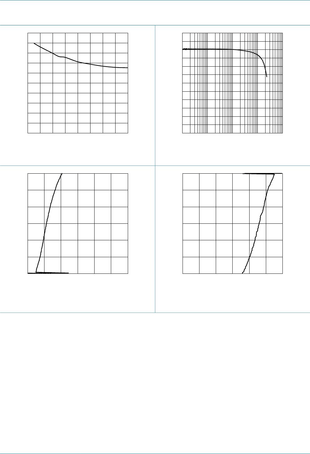
Fig. 5.
Diode capacitance as a function of frequency;
typical values
aaa-016863
f (GHz)
10
-2
10
2
10
10
-1
1
-6
-2
2
S
21
(dB)
-10
Fig. 6.
Insertion loss; typical values
V
CL
(V)
0
30
20
10
5
15
25
aaa-027608
30
I
PP
(A)
0
5
10
15
20
25
t
p
= 100 ns; Transmission Line Pulse (TLP)
Fig. 7.
Dynamic resistance with positive clamping
voltage
V
CL
(V)
-30
0
-10
-20
-25
-15
-5
aaa-027609
0
I
PP
(A)
-30
-25
-20
-15
-10
-5
t
p
= 100 ns; Transmission Line Pulse (TLP)
Fig. 8.
Dynamic resistance with negative clamping
voltage
Nexperia
PESD7V0C1BSF
Ultra low capacitance bidirectional ESD protection diode
PESD7V0C1BSF
All information provided in this document is subject to legal disclaimers.
©
Nexperia B.V. 2017. All rights reserved
Product data sheet
17 December 2017
6 / 12
50 Ω
R
d
C
s
DUT
(DEVICE
UNDER
TEST)
RG 223/U
50 Ω coax
ESD TESTER
IEC 61000-4-2 ed.2
C
s
= 150 pF; R
d
= 330 Ω
4 GHz DIGITAL
OSCILLOSCOPE
40 dB
ATTENUATOR
unclamped +8 kV ESD pulse waveform
(IEC 61000-4-2 network)
0
6
2
10
V
(kV)
-2
t (ns)
-10
70
30
4
8
40
20
10
0
50
60
unclamped -8 kV ESD pulse waveform
(IEC 61000-4-2 network)
-8
-2
-6
2
V
(kV)
-10
t (ns)
-10
70
30
-4
0
40
20
10
0
50
60
aaa-003952
Fig. 9.
ESD clamping test setup and waveforms
aaa-016866
60
80
40
20
0
100
120
V
CL
(V)
-20
t (ns)
-10
10
30
5
0
70
40
20
0
60
V
CL
at 30 ns = 4.6 V
Fig. 10.
Clamped +8 kV pulse waveform (IEC 61000-4-2
network)
aaa-016867
-40
-20
-60
-80
-100
0
20
V
CL
(V)
-120
t (ns)
-10
10
30
5
0
70
40
20
0
60
V
CL
at 30 ns = -3.8 V
Fig. 11.
Clamped -8 kV pulse waveform (IEC 61000-4-2
network)
P1-P3
P4-P6
P7-P9
P10-P12
PESD7V0C1BSFYL
Mfr. #:
Buy PESD7V0C1BSFYL
Manufacturer:
Nexperia
Description:
TVS Diodes / ESD Suppressors PESD7V0C1BSF/SOD962/SOD962
Lifecycle:
New from this manufacturer.
Delivery:
DHL
FedEx
Ups
TNT
EMS
Payment:
T/T
Paypal
Visa
MoneyGram
Western
Union
Products related to this Datasheet
PESD7V0C1BSFYL