© Semiconductor Components Industries, LLC, 2008
September, 2008 Rev. 12
1 Publication Order Number:
UC3842B/D
UC3842B, UC3843B,
UC2842B, UC2843B,
NCV3843BV
High Performance
Current Mode Controllers
The UC3842B, UC3843B series are high performance fixed
frequency current mode controllers. They are specifically designed for
OffLine and DCDC converter applications offering the designer a
costeffective solution with minimal external components. These
integrated circuits feature a trimmed oscillator for precise duty cycle
control, a temperature compensated reference, high gain error
amplifier, current sensing comparator, and a high current totem pole
output ideally suited for driving a power MOSFET.
Also included are protective features consisting of input and
reference undervoltage lockouts each with hysteresis, cyclebycycle
current limiting, programmable output deadtime, and a latch for single
pulse metering.
These devices are available in an 8pin dualinline and surface
mount (SOIC8) plastic package as well as the 14pin plastic surface
mount (SOIC14). The SOIC14 package has separate power and
ground pins for the totem pole output stage.
The UCX842B has UVLO thresholds of 16 V (on) and 10 V (off),
ideally suited for offline converters. The UCX843B is tailored for
lower voltage applications having UVLO thresholds of 8.5 V (on) and
7.6 V (off).
Features
Trimmed Oscillator for Precise Frequency Control
Oscillator Frequency Guaranteed at 250 kHz
Current Mode Operation to 500 kHz
Automatic Feed Forward Compensation
Latching PWM for CycleByCycle Current Limiting
Internally Trimmed Reference with Undervoltage Lockout
High Current Totem Pole Output
Undervoltage Lockout with Hysteresis
Low Startup and Operating Current
PbFree Packages are Available
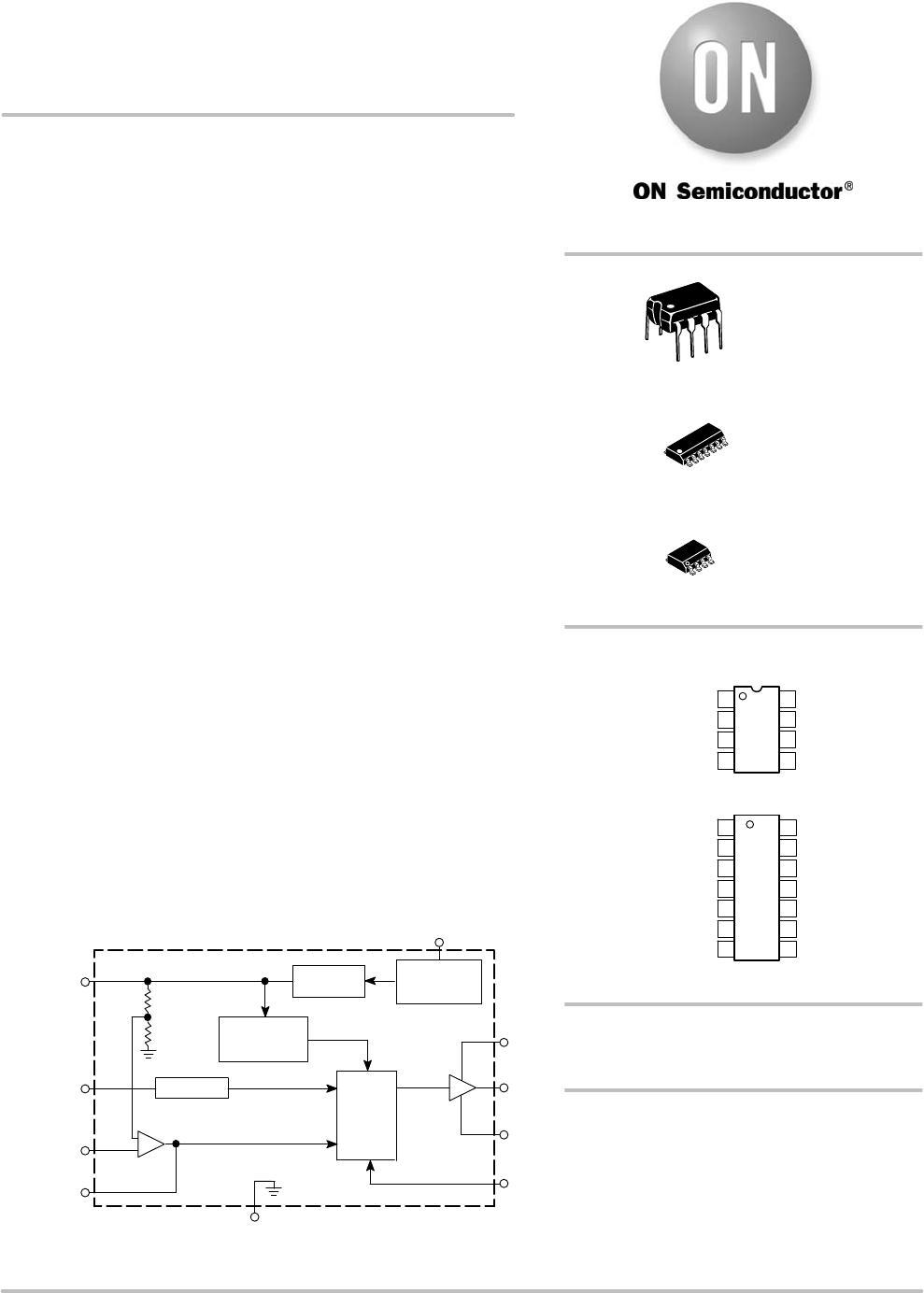
Figure 1. Simplified Block Diagram
5.0V
Reference
Latching
PWM
V
CC
Undervoltage
Lockout
Oscillator
Error
Amplifier
7(12)
V
C
7(11)
Output
6(10)
Power
Ground
5(8)
3(5)
Current
Sense
Input
V
ref
8(14)
4(7)
2(3)
1(1)
GND 5(9)
R
T
/C
T
Voltage
Feedback
Input
R
R
+
-
V
ref
Undervoltage
Lockout
Output
Compensation
Pin numbers in parenthesis are for the D suffix SOIC14 package.
V
CC
14
SOIC14
D SUFFIX
CASE 751A
1
See detailed ordering and shipping information in the package
dimensions section on page 17 of this data sheet.
ORDERING INFORMATION
See general marking information in the device marking
section on page 19 of this data sheet.
DEVICE MARKING INFORMATION
1
8
PDIP8
N SUFFIX
CASE 626
PIN CONNECTIONS
Compensation
NC
Voltage Feedback
NC
Current Sense
NC
R
T
/C
T
Compensation
Voltage Feedback
Current Sense
R
T
/C
T
V
ref
V
ref
NC
V
CC
V
C
Output
GND
Power Ground
V
CC
Output
GND
(Top View)
8
7
6
5
1
2
3
4
1
2
3
4
14
13
12
11
5
6
7
10
9
8
(Top View)
SOIC8
D1 SUFFIX
CASE 751
1
8
http://onsemi.com
UC3842B, UC3843B, UC2842B, UC2843B, NCV3843BV
http://onsemi.com
2
MAXIMUM RATINGS
Rating Symbol Value Unit
Bias and Driver Voltages (Zero Series Impedance, see also Total Device spec) V
CC
, V
C
30 V
Total Power Supply and Zener Current (I
CC
+ I
Z
) 30 mA
Output Current, Source or Sink I
O
1.0 A
Output Energy (Capacitive Load per Cycle) W 5.0
mJ
Current Sense and Voltage Feedback Inputs V
in
0.3 to + 5.5 V
Error Amp Output Sink Current I
O
10 mA
Power Dissipation and Thermal Characteristics
D Suffix, Plastic Package, SOIC14 Case 751A
Maximum Power Dissipation @ T
A
= 25°C
Thermal Resistance, JunctiontoAir
D1 Suffix, Plastic Package, SOIC8 Case 751
Maximum Power Dissipation @ T
A
= 25°C
Thermal Resistance, JunctiontoAir
N Suffix, Plastic Package, Case 626
Maximum Power Dissipation @ T
A
= 25°C
Thermal Resistance, JunctiontoAir
P
D
R
q
JA
P
D
R
q
JA
P
D
R
q
JA
862
145
702
178
1.25
100
mW
°C/W
mW
°C/W
W
°C/W
Operating Junction Temperature T
J
+150 °C
Operating Ambient Temperature
UC3842B, UC3843B
UC2842B, UC2843B
UC3842BV, UC3843BV
NCV3843BV
T
A
0 to 70
25 to + 85
40 to +105
40 to +125
°C
Storage Temperature Range T
stg
65 to +150 °C
Stresses exceeding Maximum Ratings may damage the device. Maximum Ratings are stress ratings only. Functional operation above the
Recommended Operating Conditions is not implied. Extended exposure to stresses above the Recommended Operating Conditions may affect
device reliability.
1. This device series contains ESD protection and exceeds the following tests:
Human Body Model 4000 V per JEDEC Standard JESD22-A114B
Machine Model Method 200 V per JEDEC Standard JESD22-A115-A
2. This device contains latch-up protection and exceeds 100 mA per JEDEC Standard JESD78
UC3842B, UC3843B, UC2842B, UC2843B, NCV3843BV
http://onsemi.com
3
ELECTRICAL CHARACTERISTICS (V
CC
= 15 V [Note 3], R
T
= 10 k, C
T
= 3.3 nF. For typical values T
A
= 25°C, for min/max values
T
A
is the operating ambient temperature range that applies [Note 4], unless otherwise noted.)
UC284XB UC384XB, XBV
Characteristics Symbol Min Typ Max Min Typ Max Unit
REFERENCE SECTION
Reference Output Voltage (I
O
= 1.0 mA, T
J
= 25°C) V
ref
4.95 5.0 5.05 4.9 5.0 5.1 V
Line Regulation (V
CC
= 12 V to 25 V) Reg
line
2.0 20 2.0 20 mV
Load Regulation (I
O
= 1.0 mA to 20 mA) Reg
load
3.0 25 3.0 25 mV
Temperature Stability T
S
0.2 0.2 mV/°C
Total Output Variation over Line, Load, and Temperature V
ref
4.9 5.1 4.82 5.18 V
Output Noise Voltage (f = 10 Hz to 10 kHz, T
J
= 25°C) V
n
50 50
mV
Long Term Stability (T
A
= 125°C for 1000 Hours) S 5.0 5.0 mV
Output Short Circuit Current I
SC
30 85 180 30 85 180 mA
OSCILLATOR SECTION
Frequency
T
J
= 25°C
T
A
= T
low
to T
high
T
J
= 25°C (R
T
= 6.2 k, C
T
= 1.0 nF)
f
OSC
49
48
225
52
250
55
56
275
49
48
225
52
250
55
56
275
kHz
Frequency Change with Voltage (V
CC
= 12 V to 25 V)
Df
OSC
/DV
0.2 1.0 0.2 1.0 %
Frequency Change with Temperature, T
A
= T
low
to T
high
Df
OSC
/DT
1.0 0.5 %
Oscillator Voltage Swing (PeaktoPeak) V
OSC
1.6 1.6 V
Discharge Current (V
OSC
= 2.0 V)
T
J
= 25°C, T
A
= T
low
to T
high
UC284XB, UC384XB
T
A
= T
low
to T
high
UC384XBV
I
dischg
7.8
7.5
8.3
8.8
8.8
7.8
7.6
7.2
8.3
8.8
8.8
8.8
mA
ERROR AMPLIFIER SECTION
Voltage Feedback Input (V
O
= 2.5 V) V
FB
2.45 2.5 2.55 2.42 2.5 2.58 V
Input Bias Current (V
FB
= 5.0 V) I
IB
0.1 1.0 0.1 2.0
mA
Open Loop Voltage Gain (V
O
= 2.0 V to 4.0 V) A
VOL
65 90 65 90 dB
Unity Gain Bandwidth (T
J
= 25°C) BW 0.7 1.0 0.7 1.0 MHz
Power Supply Rejection Ratio (V
CC
= 12 V to 25 V) PSRR 60 70 60 70 dB
Output Current
Sink (V
O
= 1.1 V, V
FB
= 2.7 V)
Source (V
O
= 5.0 V, V
FB
= 2.3 V)
I
Sink
I
Source
2.0
0.5
12
1.0
2.0
0.5
12
1.0
mA
Output Voltage Swing
High State (R
L
= 15 k to ground, V
FB
= 2.3 V)
Low State (R
L
= 15 k to V
ref
, V
FB
= 2.7 V)
UC284XB, UC384XB
UC384XBV
V
OH
V
OL
5.0
6.2
0.8
1.1
5.0
6.2
0.8
0.8
1.1
1.2
V
CURRENT SENSE SECTION
Current Sense Input Voltage Gain (Notes 5 and 6)
UC284XB, UC384XB
UC384XBV
A
V
2.85
3.0
3.15
2.85
2.85
3.0
3.0
3.15
3.25
V/V
Maximum Current Sense Input Threshold (Note 5)
UC284XB, UC384XB
UC384XBV
V
th
0.9
1.0
1.1
0.9
0.85
1.0
1.0
1.1
1.1
V
Power Supply Rejection Ratio (V
CC
= 12 V to 25 V, Note 5) PSRR 70 70 dB
Input Bias Current I
IB
2.0 10 2.0 10
mA
Propagation Delay (Current Sense Input to Output) t
PLH(In/Out)
150 300 150 300 ns
3. Adjust V
CC
above the Startup threshold before setting to 15 V.
4. Low duty cycle pulse techniques are used during test to maintain junction temperature as close to ambient as possible.
T
low
= 0°C for UC3842B, UC3843B; 25°C for UC2842B, UC2843B; 40°C for UC3842BV, UC3843BV
T
high
= +70°C for UC3842B, UC3843B; +85°C for UC2842B, UC2843B; +105°C for UC3842BV, UC3843BV
NCV3843BV: T
low
= 40°C, T
high
= +125°C. Guaranteed by design. NCV prefix is for automotive and other applications requiring site and
change control.
5. This parameter is measured at the latch trip point with V
FB
= 0 V.
6. Comparator gain is defined as: A
V
DV Output Compensation
DV Current Sense Input

UC3842BN

Mfr. #:
Manufacturer:
STMicroelectronics
Description:
Switching Controllers 0.5mA Current Mode
Lifecycle:
New from this manufacturer.
Delivery:
DHL FedEx Ups TNT EMS
Payment:
T/T Paypal Visa MoneyGram Western Union