DocID7699 Rev 9 5/15
T4 series Characteristics
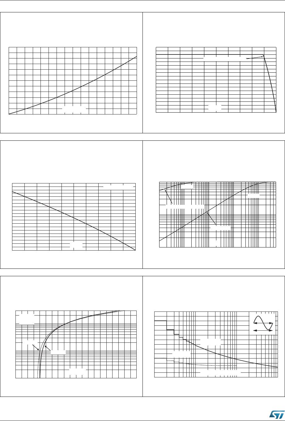
Figure 7. Non-repetitive surge peak on-state
current for a sinusoidal pulse
with width t
p
< 10 ms
Figure 8. Relative variation of gate trigger
current, holding current and latching current
versus junction temperature (typical values)
W
S
PV
,
760
$
,
760
7
M
LQLWLDO &
GOGWOLPLWDWLRQ
$V
-40 -20 0 20 40 60 80 100 120 140
0.0
0.5
1.0
1.5
2.0
2.5
T (°C)
j
I,I,I[T] /
GTHL j
I ,I ,I [T =25°C]
GTHL j
I
GT
I
H
& I
L
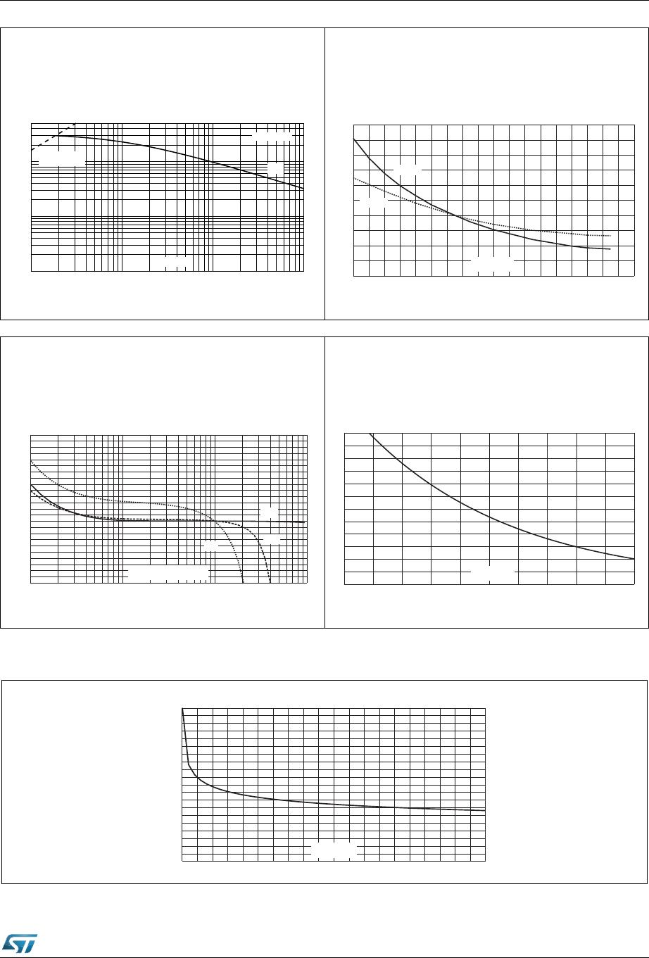
Figure 9. Relative variation of critical rate of
decrease of main current versus (dV/dt)c
(typical values)
Figure 10. Relative variation of critical rate of
decrease of main current versus junction
temperature
Figure 11. DPAK thermal resistance junction to ambient versus copper surface under tab (printed
circuit board FR4, copper thickness: 35 µm)
0.1 1.0 10.0 100.0
0.0
0.2
0.4
0.6
0.8
1.0
1.2
1.4
1.6
1.8
2.0
2.2
2.4
(dV/dt)c (V/µs)
(dI/dt)c [(dV/dt)c] / Specified (dI/dt)c
T405
T435
T410
0 25 50 75 100 125
0
1
2
3
4
5
6
(dI/dt)c [T ] / pecified]
j
(dI/dt)c [T s
j
T (°C)
j
0 4 8 1216202428323640
0
10
20
30
40
50
60
70
80
90
100
S(cm²)
R (°C/W)
th(j-a)