Electrical specifications L9953 / L9953XP
14/38 Doc ID 14278 Rev 4
2.5 SPI - electrical characteristics
(V
S
= 8 to 16V, V
CC
= 4.5 to 5.3V, T
j
= - 40 to 150°C, unless otherwise specified. The
voltages are referred to GND and currents are assumed positive, when the current flows into
the pin).
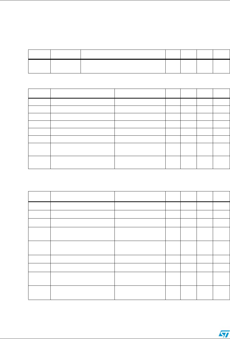
Table 12. Delay time from standby to active mode
Symbol Parameter Test condition Min. Typ. Max. Unit
t
set
Delay time
Switching from standby to active mode.
Time until output drivers are enabled
160 300 µs
Table 13. Inputs: CSN, CLK, PWM1/2 and DI
Symbol Parameter Test condition Min. Typ. Max. Unit
V
inL
Input low level V
CC
= 5V 1.5 2.0 V
V
inH
Input high level V
CC
= 5V 3.0 3.5 V
V
inHyst
Input hysteresis V
CC
= 5V 0.5 V
I
CSN in
Pull up current at input CSN V
CSN
= 3.5V V
CC
= 5V -40 -20 -5 µA
I
CLK in
Pull down current at input CLK V
CLK
= 1.5V 10 25 50 µA
I
DI in
Pull down current at input DI V
DI
= 1.5V 10 25 50 µA
I
PWM1 in
Pull down current at input
PWM1
V
PWM
= 1.5V 10 25 50 µA
C
in
(1)
1. Value of input capacity is not measured in production test. Parameter guaranteed by design.
Input capacitance at input
CSN, CLK, DI and PWM1/2
0 V < V
CC
< 5.3V 10 15 pF
Table 14. DI timing
(1)
1. DI timing parameters tested in production by a passed / failed test:
Tj= -40°C / +25°C: SPI communication @ 2MHz.
Tj= +125°C SPI communication @ 1.25 MHz.
Symbol Parameter Test condition Min. Typ. Max. Unit
t
CLK
Clock period V
CC
= 5V 1000 ns
t
CLKH
Clock high time V
CC
= 5V 400 ns
t
CLKL
Clock low time V
CC
= 5V 400 ns
t
set CSN
CSN setup time, CSN low
before rising edge of CLK
V
CC
= 5V 400 ns
t
set CLK
CLK setup time, CLK high
before rising edge of CSN
V
CC
= 5V 400 ns
t
set DI
DI setup time V
CC
= 5V 200 ns
t
hold time
DI hold time V
CC
= 5V 200 ns
t
r in
Rise time of input signal DI,
CLK, CSN
V
CC
= 5V 100 ns
t
f in
Fall time of input signal DI,
CLK, CSN
V
CC
= 5V 100 ns

