LTC2942-1
13
29421f
applicaTions inFormaTion
1000h at 1A current and 85°C ambient temperature; this
outperforms most types of discrete sense resistors except
those of the very high and ultrahigh stability variety. See
the Typical Performance Characteristics for expected
resistor drift performance under worst-case conditions.
Drift will be much slower at lower temperatures. Contact
LTC applications for more information.
For most coulomb counter applications this aging behavior
of the integrated sense resistor is insignificant compared
to the change of battery capacity due to battery aging.
The LTC2942-1 is factory trimmed to optimum accuracy
when new; for applications which require the best possible
coulomb count accuracy over the full product lifetime, the
coulomb counter gain can be adjusted in software. For
instance, if the error contribution of sense resistor drift
must be limited to ±1%, coulomb counts may be biased
high by 1% (use factor 1.01), and maximum operational
temperature and current then must be derated such that
sense resistor drift over product lifetime or calibration
intervals is less than –2%.
Applications employing the standard external resistor
LTC2942 with an external 50mΩ sense resistor may be
upgraded to the pin-compatible LTC2942-1 by removing
the external sense resistor.
Voltage Drop Between SENSE
+
and SENSE
The LTC2942-1 is trimmed for an effective internal resis-
tance of 50mΩ , but the total pin-to-pin resistance (R
PP
),
consisting of the sense resistor in series with pin and bond
wire resistances, is somewhat higher. Assuming a sense
resistor temperature coefficient of about 3900ppm/K,
the total resistance between SENSE
+
and SENSE
at a
temperature T is typically:
R
PP
(T) = R
PP(TNOM)
[1 + 0.0039(T – T
NOM
)]
SCL
SDA
START
CONDITION
STOP
CONDITION
ADDRESS R/W ACK DATA ACK DATA ACK
1 - 7 8 9
29421 F03
a6 - a0 b7 - b0 b7 - b0
1 - 7 8 9 1 - 7 8 9
P
S
Figure 3. Data Transfer Over I
2
C or SMBus
FROM MASTER TO SLAVE
S W
ADDRESS REGISTER DATA
FROM SLAVE TO MASTER
29421 F04
A: ACKNOWLEDGE (LOW)
A: NOT ACKNOWLEDGE (HIGH)
S: START CONDITION
P: STOP CONDITION
R: READ BIT (HIGH)
W: WRITE BIT (LOW)
A A A
0
1100100 01h FCh
0 0 0
P
Figure 4. Writing FCh to the LTC2942-1 Control Register (B)
S W
ADDRESS REGISTER DATA
29421 F05
A A A
0
1100100 02h F0h 01h
0 0 0
0
P
DATA
A
S W
ADDRESS REGISTER S
29421 F06
A A ADDRESS
0
1100100 00h 1
0 0 1100100
0
P
R
1
A
01h
DATA
A
Figure 5. Writing F001h to the LTC2942-1
Accumulated Charge Register (C, D)
Figure 6. Reading the LTC2942-1 Status Register (A)
S W
ADDRESS REGISTER S
29421 F07
A A ADDRESS
0
1100100 08h 1
0 0 1100100
0
P
R
0
A
F1h
DATA
24h
DATA
A
1
A
Figure 7. Reading the LTC2942-1 Voltage Register (I, J)
LTC2942-1
14
29421f
applicaTions inFormaTion
where T
NOM
= 27°C (or 300K) and R
PP
(T
NOM
) is from
the Electrical Characteristics table. This means that the
resistance between SENSE
+
and SENSE
may drop by
26% if die temperature changes from 27°C to –40°C
or increase by 23% for a 27°C to 85°C die temperature
change. Ensure that total voltage drop between SENSE
+
and SENSE
, caused by maximum peak current flowing
in/out of SENSE
:
V
DROP
= I
PEAK
• R
PP
(T
DIE(MAX)
)
does not exceed the application’s requirements.
Limiting Inrush Current
Inrush currents during events like battery insertion or
closure of a mechanical power switch may be substan-
tially higher than peak currents during normal operation.
Extremely large inrush currents may require additional
circuitry to keep currents through the LTC2942-1 sense
resistor below the absolute maximum ratings.
Note that external Schottky clamp diodes between SENSE
+
and SENSE
can leak significantly, especially at high tem-
perature, which can cause significant coulomb counter
errors. Preferred solutions to limit inrush current include
active Hot Swap™ current limiting or connector designs
that include current limiting resistance and staggered pins
to ensure a low impedance connection when the connector
is fully mated.
Power Dissipation
Power dissipation in the R
PP
resistance when operated
at high currents can increase the die temperature sev-
eral degrees over ambient. Soldering the exposed pad
of the DFN package to a large copper region on the PCB
is recommended for applications operating close to the
specified maximum current and ambient temperature. Die
temperature at a given I
SENSE
can be estimated by:
T
DIE
= T
AMB
+ 1.22 • θ
JA
• R
PP(MAX)
• I
SENSE
2
where the factor 1.22 approximates the effect of sense
resistor self-heating, R
PP(MAX)
is the maximum pad-to-
pad resistance at nominal temperature (27°C) and θ
JA
is
the thermal resistance from junction to ambient. The θ
JA
data given for the DFN package is valid for typical PCB
layouts; more precise θ
JA
data for a particular PCB layout
may be obtained by measuring the voltage V
P-P
between
SENSE
+
and SENSE
, the ambient temperature T
AMB
, and
the die temperature T
DIE
, and calculating:
θ
JA
DIE AMB
P P SENSE
T T
V I
=
-
Both T
AMB
and T
DIE
temperature may be measured using
the internal temperature sensor included in the LTC2942-1.
I
SENSE
should be set to zero to measure T
AMB
, and high
enough during T
DIE
measurement to achieve a significant
temperature increase over T
AMB
.
S R
ALERT RESPONSE ADDRESS DEVICE ADDRESS
29421 F08
A
1
0001100 11001001
0 1
P
A
Figure 8. LTC2942-1 Serial Bus SDA Alert Response Protocol
S10ms W
ADDRESS REGISTER S
29421 F09
A A ADDRESS
0
1100100 08h 1
0 0 1100100
0
P
R
0
A
F1h
DATA
80h
DATA
A
1
A
S W
ADDRESS REGISTER DATA
A A
0
1100100 01h BC
0 0
P
Figure 9. Voltage Conversion Sequence
S W
ADDRESS REGISTER S
29421 F10
A A ADDRESS
0
1100100 02h 1
0 0 1100100
0
P
R
0
A
80h
DATA
01h
DATA
A
1
A
Figure 10. Reading the LTC2942-1 Accumulated Charge Registers (C, D)
LTC2942-1
15
29421f
Information furnished by Linear Technology Corporation is believed to be accurate and reliable.
However, no responsibility is assumed for its use. Linear Technology Corporation makes no representa-
tion that the interconnection of its circuits as described herein will not infringe on existing patent rights.
package DescripTion
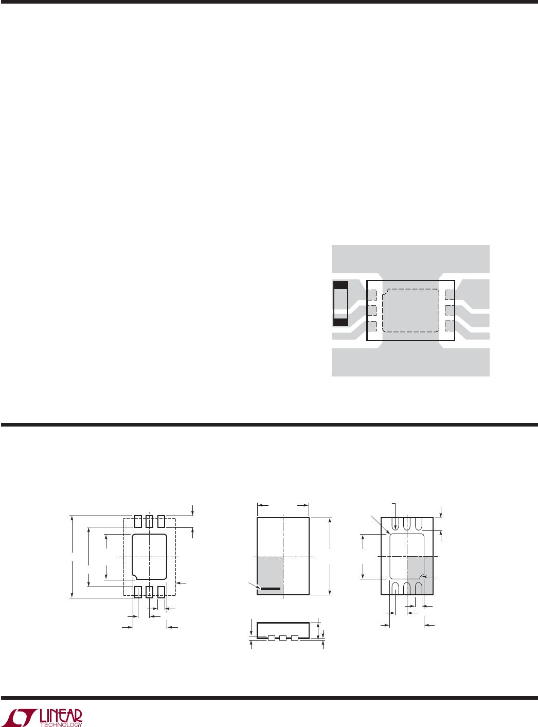
Figure 11. Recommended Layout
DCB Package
6-Lead Plastic DFN (2mm × 3mm)
(Reference LTC DWG # 05-08-1715)
3.00 p0.10
(2 SIDES)
2.00 p0.10
(2 SIDES)
NOTE:
1. DRAWING TO BE MADE A JEDEC PACKAGE OUTLINE M0-229 VARIATION OF (TBD)
2. DRAWING NOT TO SCALE
3. ALL DIMENSIONS ARE IN MILLIMETERS
4. DIMENSIONS OF EXPOSED PAD ON BOTTOM OF PACKAGE DO NOT INCLUDE
MOLD FLASH. MOLD FLASH, IF PRESENT, SHALL NOT EXCEED 0.15mm ON ANY SIDE
5. EXPOSED PAD SHALL BE SOLDER PLATED
6. SHADED AREA IS ONLY A REFERENCE FOR PIN 1 LOCATION ON THE
TOP AND BOTTOM OF PACKAGE
0.40 p 0.10
BOTTOM VIEW—EXPOSED PAD
1.65 p 0.10
(2 SIDES)
0.75 p0.05
R = 0.115
TYP
R = 0.05
TYP
1.35 p0.10
(2 SIDES)
1
3
64
PIN 1 BAR
TOP MARK
(SEE NOTE 6)
0.200 REF
0.00 – 0.05
(DCB6) DFN 0405
0.25 p 0.05
0.50 BSC
PIN 1 NOTCH
R0.20 OR 0.25
s 45o CHAMFER
0.25 p 0.05
1.35 p0.05
(2 SIDES)
RECOMMENDED SOLDER PAD PITCH AND DIMENSIONS
1.65 p0.05
(2 SIDES)
2.15 p0.05
0.70 p0.05
3.55 p0.05
PACKAGE
OUTLINE
0.50 BSC
Measuring Current
In some applications, it may be desirable to measure the
current I
SENSE
flowing through the internal sense resistor.
Since charge measured by the coulomb counter is the
time integral over I
SENSE
, differentiation of the contents
of the accumulated charge register (ACR) over time may
be used to measure average current.
Accuracy of such an indirect current measurement is limited
by the basic accuracy of the coulomb counter, the accuracy
of the timebase within the host system, quantization caused
by the prescaler setting, and time delays caused by I
2
C
transactions. Still, especially at higher currents, useful
results may be obtained by reading the accumulated charge
register twice, with a defined time interval in between, and
dividing the charge difference by the time interval. The
time interval may be increased at low currents to limit time
quantization errors to the desired accuracy. For quicker
current measurements at low currents, prescale factor M
may be temporarily decreased, sacrificing some coulomb
count accuracy for higher current resolution.
Extending Coulomb Counter Range
To increase the range of the coulomb counter for battery
capacities higher than 5.5Ah, the host controller can either
regularly poll the accumulated charge register (ACR) or use
the threshold registers to determine when the accumulated
charge register approaches the minimum or maximum
limits. At this point it can add or subtract a fixed charge
quantity and rewrite the result into the ACR. The added
or subtracted charge quantities can then be tracked in
software, increasing the effective ACR range.
PC Board Layout Suggestions
Keep all traces as short as possible to minimize noise and
inaccuracy. Use wider traces from the resistor to the bat-
tery, load and/or charger (see Figure 11). Put the bypass
capacitor close to SENSE
+
and GND. Provide adequate
copper area on exposed pad for heat sinking.
LTC2942-1
ELECTRICALLY ISOLATED HEAT SINK
CONNECTED TO EXPOSED PAD ONLY
29421 F11
TO BATTERY
TO
CHARGER/LOAD
4
5
6
3
2
1
C
applicaTions inFormaTion

LTC2942IDCB-1#TRMPBF

Mfr. #:
Manufacturer:
Analog Devices / Linear Technology
Description:
Battery Management Battery Gas Gauge with Temperature & Voltage Measurement and Internal Sense Resistor
Lifecycle:
New from this manufacturer.
Delivery:
DHL FedEx Ups TNT EMS
Payment:
T/T Paypal Visa MoneyGram Western Union