DATASHEET
QUADRACLOCK QUADRATURE DELAY BUFFER ICS672-01/02
IDT™ / ICS™
QUADRACLOCK QUADRATURE DELAY BUFFER 1
ICS672-01/02 REV L 051310
Description
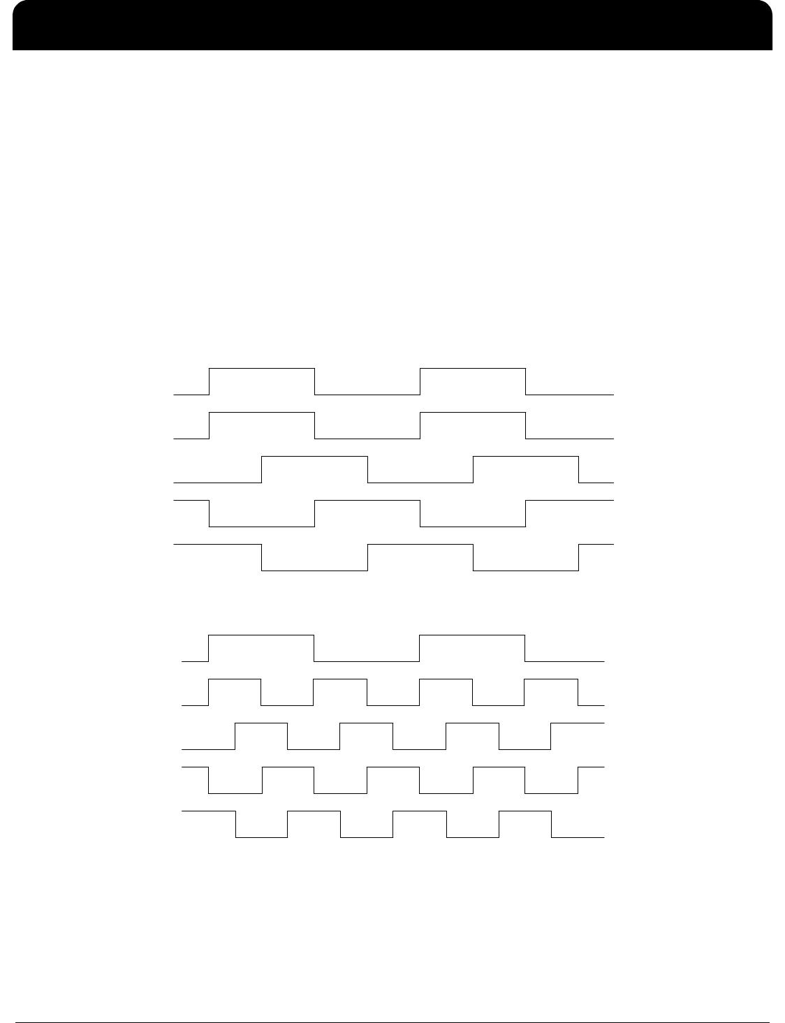
The ICS672-01/02 are zero delay buffers that generate four
output clocks whose phases are spaced at 90° intervals.
Based on IDT’s proprietary low jitter Phase-Locked Loop
(PLL) techniques, each device provides five low-skew
outputs, with clock rates up to 84 MHz for the ICS672-01
and up to 135 MHz for the ICS672-02. By providing outputs
delayed one quarter clock cycle, the device is useful for
systems requiring early or late clocks. The ICS672-01/02
include multiplier selections of x0.5, x1, x2, x3, x4, x5, or x6.
They also offer a mode to power-down all internal circuitry
and tri-state the outputs. In normal operation, output clock
FBCLK is tied to the FBIN pin.
IDT manufactures the largest variety of clock generators
and buffers, and is the largest clock supplier in the world.
Features
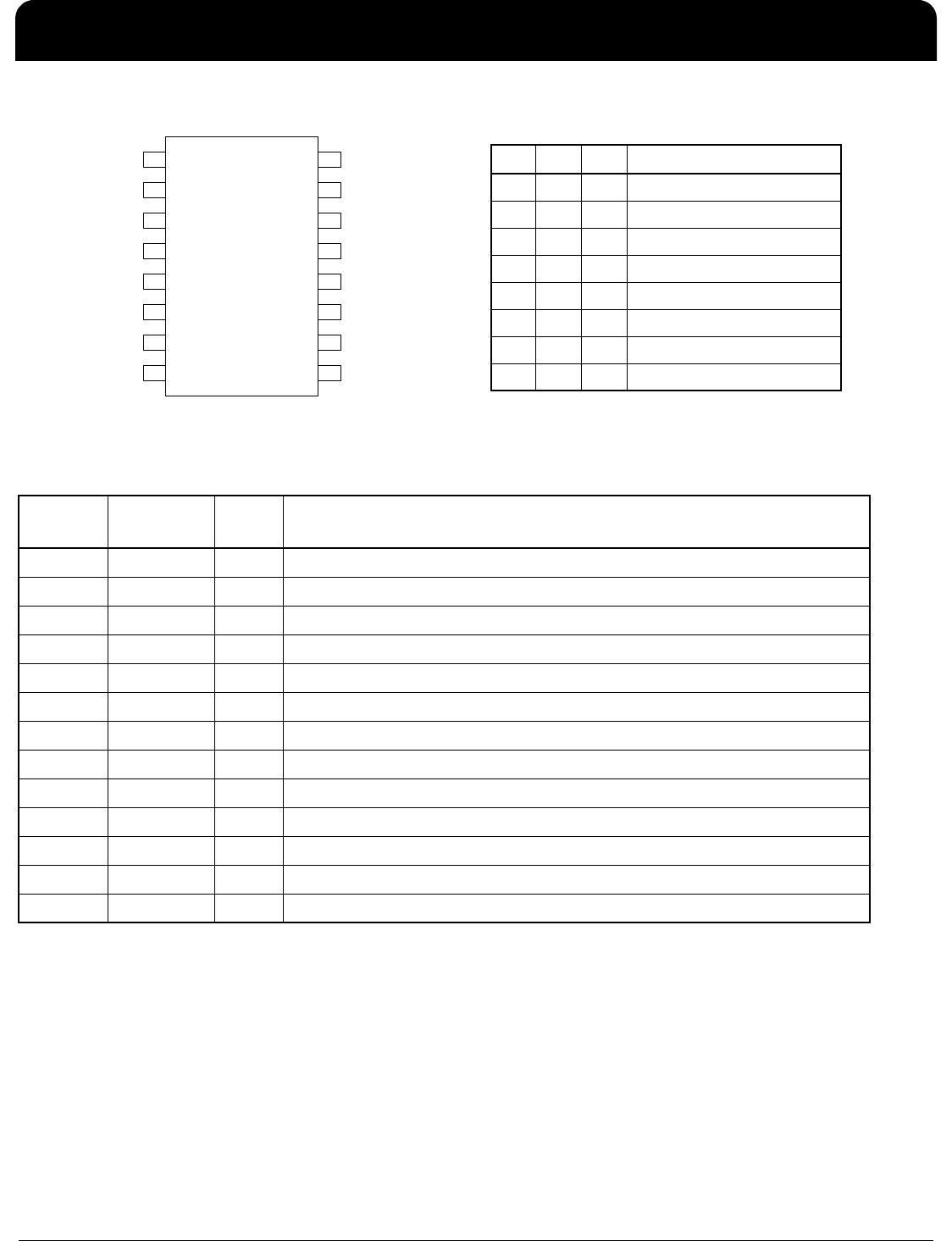
• Packaged in 16-pin SOIC
• Pb (lead) free package, RoHS compliant
• Input clock range from 5 MHz to 150 MHz (depends on
multiplier)
• Clock outputs from up to 84 MHz (ICS672-01) and up to
135 MHz (ICS672-02)
• Zero input-output delay
• Integrated x0.5, x1, x2, x3, x4, x5, or x6 selections
• Four accurate (<250 ps) outputs with 0°, 90°, 180°, and
270° phase shift from ICLK, and one FBCLK (0°)
• Separate supply for output clocks from 2.5 V to 5 V
• Full CMOS outputs (TTL compatible)
• Tri-state mode for board-level testing
• Includes Power-down for power savings
• Advanced, low power, sub-micron CMOS process
• 3.3 V to 5 V operating voltage
• Industrial temperature version available
Block Diagram
Control
Logic
CLK0
VDDIO
PLL
Multiplier
and
Quadrature
Generation
FBIN
S2:S0
IN
CLKFB
3
Power Down plus Tri-state
VDD
2
External
Feedback
GND
3
CLK90
CLK180
CLK270