LT3007 Series
10
3007fa
For more information www.linear.com/LT3007
APPLICATIONS INFORMATION
The LT3007 is a low dropout linear regulator with ultra-
low quiescent current and shutdown. Quiescent current is
extremely low at 3µA and drops well below 1µA in shut
-
down. The device supplies up to 20mA of output current.
Dropout voltage at 20mA is typically 300mV. The LT3007
incorporates several protection features, making it ideal for
use in battery-powered systems. The device protects itself
against both reverse-input and reverse-output voltages.
In battery backup applications, where a backup battery
holds up the output when the input is pulled to ground,
the LT3007 acts as if a blocking diode is in series with its
output and prevents reverse current flow. In applications
where the regulator load returns to a negative supply, the
output can be pulled below ground by as much as 50V
without affecting start-up or normal operation.
Care must be taken when designing LT3007 applications
to operate at temperatures greater than 125°C. See the
High Temperature Operation Section for more information.
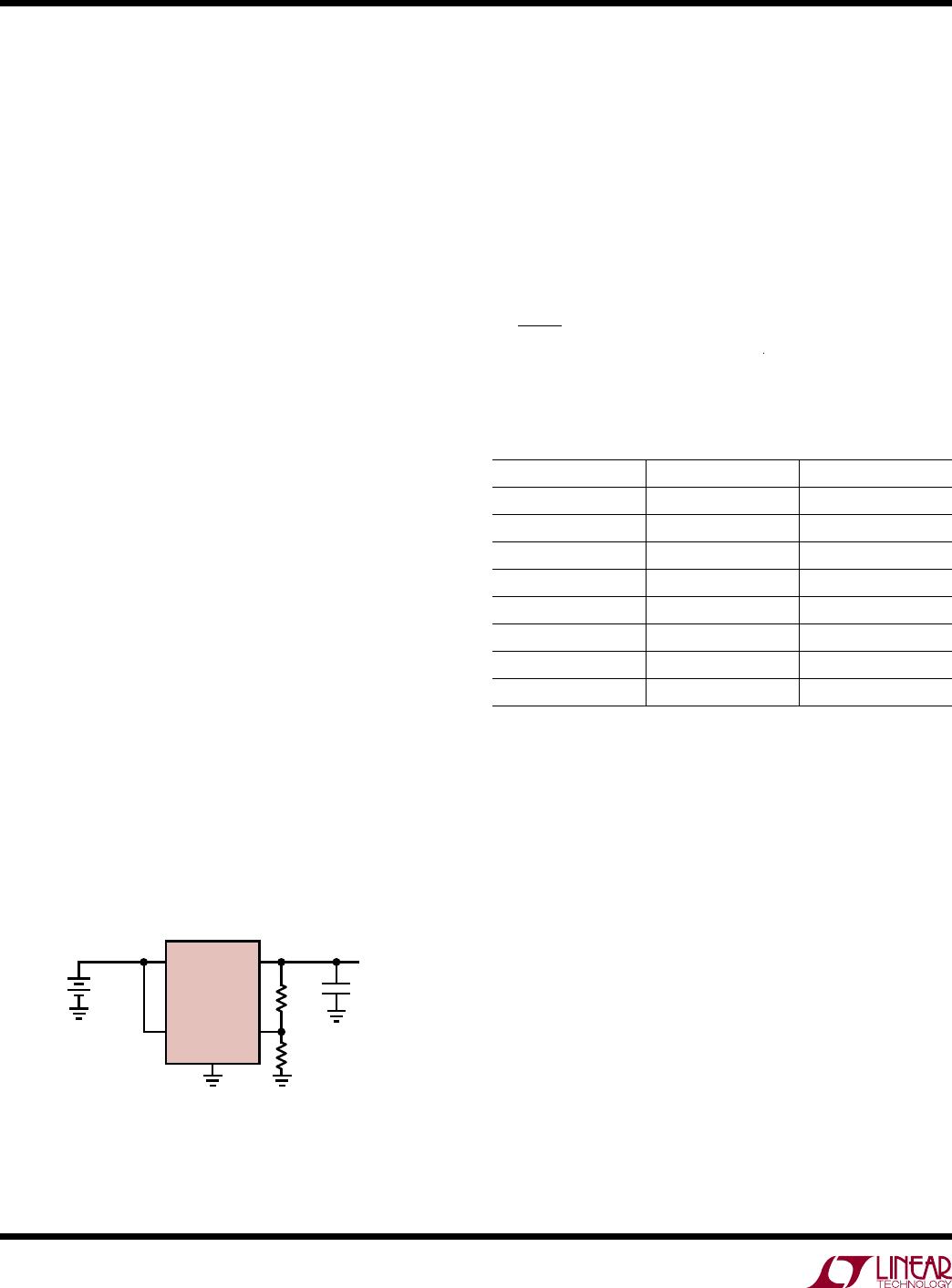
Adjustable Operation
The LT3007 has an output voltage range of 0.6V to 44.5V.
Figure 2 shows that output voltage is set by the ratio of two
external resistors. The IC regulates the
output to maintain the
ADJ pin voltage at 600mV referenced to ground. The current
in R1 equals 600mV/R1 and the current in R2 is the current
in R1 minus the ADJ pin bias current. The ADJ pin bias cur
-
rent, typically 400
pA at 25°C, flows out of the pin. Calculate
the output voltage using the formula in Figure 2. An R1 value
of 619k sets the divider current to 0.97µA. Do not make R1’s
value any greater than 619k to minimize output voltage errors
due to the ADJ pin bias current and to insure stability under
minimum load conditions. In shutdown, the output turns off
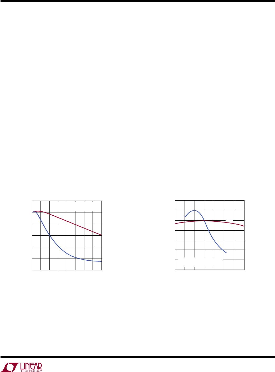
and the divider current is zero. Curves of ADJ Pin Voltage vs
Temperature and ADJ Pin Bias Current vs Temperature appear
in the Typical Performance Characteristics.
Specifications for output voltages greater than 0.6V are
proportional to the ratio of the desired output voltage to
0.6V: V
OUT
/0.6V. For example, load regulation for an output
current change of 100µA to 20mA is –0.5mV typical at
V
OUT
= 0.6V. At V
OUT
= 5V, load regulation is:
• (−0.5mV) = −4.17mV
Table 1 shows resistor divider values for some common
output voltages with a resistor divider current of about 1µA.
Figure 2. Adjustable Operation
Table 1. Output Voltage Resistor Divider Values
V
OUT
R1 R2
1V 604k 402k
1.2V 590k 590k
1.5V 590k 887k
1.8V 590k 1.18M
2.5V 590k 1.87M
3V 590k 2.37M
3.3V 619k 2.8M
5V 590k 4.32M
IN
SHDN
R2
R1
3007 F02
OUT
V
IN
V
OUT
= 600mV • (1 + R2/R1) – (I
ADJ
• R2)
V
ADJ
= 600mV
I
ADJ
= 0.4nA at 25°C
OUTPUT RANGE = 0.6V to 44.5V
ADJ
GND
LT3007
V
OUT
Because the ADJ pin is relatively high impedance (de-
pending on the
resistor divider used), stray capacitances
at this pin should be minimized. Special attention should
be given to any stray capacitances that can couple ex
-
ternal signals onto the ADJ pin, producing undesirable
output transients or ripple.
Extra care should be taken in assembly when using high
valued resistors. Small amounts of board contamination
can lead to significant shifts in output voltage. Appropriate
post-assembly board cleaning measures should be
implemented to prevent board contamination. If the
board is to be subjected to humidity cycling or if board
cleaning measures cannot be guaranteed, consideration
should be given to using resistors an order of magnitude
smaller than in Table 1 to prevent contamination from
causing unwanted shifts in the output voltage. A fixed
voltage option in the LT3007 series does not need these
special considerations.