2
COMMERCIAL/INDUSTRIAL TEMPERATURE RANGES
IDT74FCT3807/A
3.3V CMOS 1-TO-10 CLOCK DRIVER
NOTES:
1. For conditions shown as Max. or Min., use appropriate value specified under Electrical Characteristics for the applicable device type.
2. Typical values are at VCC = 3.3V, +25°C ambient.
3. Per TTL driven input (VIN = VCC -0.6V); all other inputs at VCC or GND.
4. This parameter is not directly testable, but is derived for use in Total Power Supply calculations.
5. Values for these conditions are examples of the IC formula. These limits are guaranteed but not tested.
6. IC = IQUIESCENT + IINPUTS + IDYNAMIC
IC = ICC + ΔICC DHNT + ICCD (fi)
ICC = Quiescent Current (ICCL, ICCH and ICCZ)
ΔICC = Power Supply Current for a TTL High Input (VIN = VCC -0.6V)
DH = Duty Cycle for TTL Inputs High
NT = Number of TTL Inputs at DH
ICCD = Dynamic Current Caused by an Input Transition Pair (HLH or LHL)
fi = Input Frequency
All currents are in milliamps and all frequencies are in megahertz.
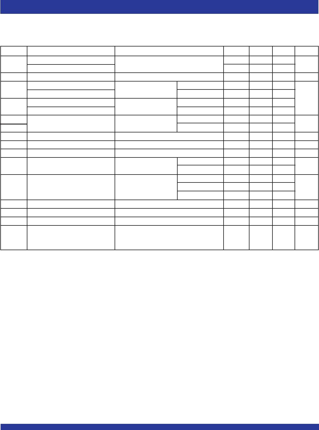
ABSOLUTE MAXIMUM RATINGS
(1)
Symbol Description Max Unit
VTERM
(2)
Terminal Voltage with Respect to GND –0.5 to +4.6 V
VTERM
(3)
Terminal Voltage with Respect to GND –0.5 to +7 V
VTERM
(4)
Terminal Voltage with Respect to GND –0.5 to VCC+0.5 V
TSTG Storage Temperature –65 to +150 ° C
IOUT DC Output Current –60 to +60 mA
NOTES:
1. Stresses greater than those listed under ABSOLUTE MAXIMUM RATINGS may cause
permanent damage to the device. This is a stress rating only and functional operation
of the device at these or any other conditions above those indicated in the operational
sections of this specification is not implied. Exposure to absolute maximum rating
conditions for extended periods may affect reliability.
2. VCC terminals.
3. Input terminals.
4. Outputs and I/O terminals.
CAPACITANCE (TA = +25
O
C, f = 1.0MHz)
Symbol Parameter
(1)
Conditions Typ. Max. Unit
CIN Input Capacitance VIN = 0V 4.5 6 pF
C
OUT Output Capacitance VOUT = 0V 5.5 8 pF
NOTE:
1. This parameter is measured at characterization but not tested.
PIN DESCRIPTION
Pin Names Description
IN Clock Inputs
O x Clock Outputs
POWER SUPPLY CHARACTERISTICS
Symbol Parameter Test Conditions
(1)
Min. Typ.
(2)
Max. Unit
ΔICC Quiescent Power Supply Current VCC = Max. — 10 30 μA
TTL Inputs HIGH VIN = VCC –0.6V
(3)
ICCD Dynamic Power Supply Current
(4)
VCC = Max. VIN = VCC — 0.31 0.45 mA/
Input toggling VIN = GND MHz
50% Duty Cycle
Outputs Open
IC Total Power Supply Current
(6)
VCC = Max. VIN = VCC — 15.5 22.8 mA
Input toggling VIN = GND
50% Duty Cycle
Outputs Open VIN = VCC –0.6V — 15.5 22.8
fi = 50MHz VIN = GND