©2011 Silicon Storage Technology, Inc. DS25028A 08/11
21
16 Mbit / 32 Mbit Multi-Purpose Flash Plus
SST39VF1601 / SST39VF3201
SST39VF1602 / SST39VF3202
Not Recommended for New Designs
Microchip Technology Company
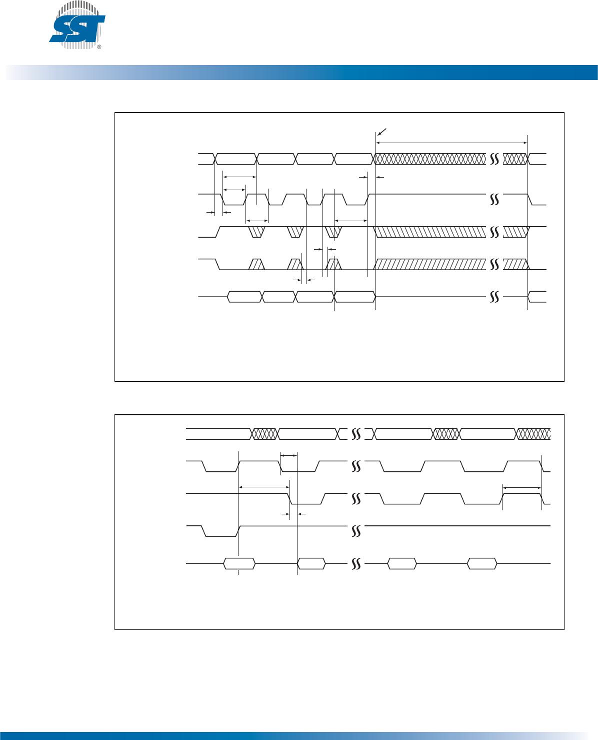
Figure 10:WE# Controlled Block-Erase Timing Diagram
Figure 11:WE# Controlled Sector-Erase Timing Diagram
1223 F09.5
ADDRESS A
MS-0
DQ
15-0
WE#
SW0 SW1 SW2 SW3 SW4 SW5
5555 2AAA 2AAA5555 5555
XX55 XX50XX55XXAA XX80 XXAA
BA
X
OE#
CE#
SIX-BYTE CODE FOR BLOCK-ERASE
T
BE
T
WP
Note: This device also supports CE# controlled Block-Erase operation. The WE# and CE# signals are
interchageable as long as minimum timings are met. (See Table 17)
BA
X
= Block Address
A
MS
= Most significant address
A
MS
=A
19
for SST39VF1601/1602 and A
20
for SST39VF3201/3202
WP# must be held in proper logic state (V
IL
or V
IH
) 1 µs prior to and 1 µs after the command sequence
X can be V
IL
or V
IH,
but no other value
1223 F10.5
ADDRESS A
MS-0
DQ
15-0
WE#
SW0 SW1 SW2 SW3 SW4 SW5
5555 2AAA 2AAA5555 5555
XX55 XX30XX55XXAA XX80 XXAA
SA
X
OE#
CE#
SIX-BYTE CODE FOR SECTOR-ERASE
T
SE
T
WP
Note: This device also supports CE# controlled Sector-Erase operation. The WE# and CE# signals are
interchageable as long as minimum timings are met. (See Table 17)
SA
X
= Sector Address
A
MS
= Most significant address
A
MS
=A
19
for SST39VF1601/1602 and A
20
for SST39VF3201/3202
WP# must be held in proper logic state (V
IL
or V
IH
) 1 µs prior to and 1 µs after the command sequence
X can be V
IL
or V
IH
, but no other value