IDT
®
Four Output Low Power Differential Buffer for PCI Express for Gen1, Gen2, Gen3, and QPI 1645F—08/16/13
Advance Information
9DBL411B
Four Output Low Power Differential Buffer for PCI Express Gen1, Gen2, Gen3, and QPI
6
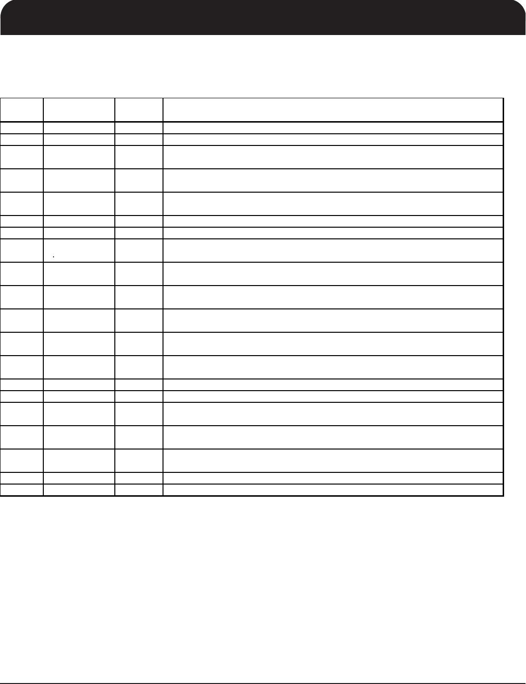
AC Electrical Characteristics - DIF Low Power Differential Outputs
PARAMETER SYMBOL CONDITIONS MIN MAX UNITS NOTES
Rising Edge Slew Rate t
SLR
Differential Measurement 1.5 4 V/ns 1,2
Falling Edge Slew Rate t
FLR
Differential Measurement 1.5 4 V/ns 1,2
Slew Rate Variation t
SLVAR
Single-ended Measurement 20 % 1
Maximum Output Voltage V
HIGH
Includes overshoot 1150 mV 1
Minimum Output Voltage V
LOW
Includes undershoot -300 mV 1
Differential Voltage Swing V
SWING
Differential Measurement 1200 mV 1
Crossing Point Voltage V
XABS
Single-ended Measurement 300 550 mV 1,3,4
Crossing Point Variation V
XABSVAR
Single-ended Measurement 140 mV 1,3,5
Duty Cycle Distortion D
CYCDIS0
Differential Measurement,
fIN<=133.33MHz
3%1,6
Additive Cycle to Cycle
Jitter
DIFJ
C2CADD
Differential Measurement,
Additive
15 ps 1
DIF[3:0] Skew DIF
SKEW
Differential Measurement 50 ps 1
Propagation Delay t
PD
Input to output Delay 2.5 3.5 ns 1
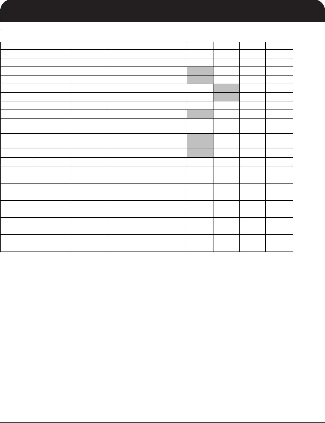
Additive Phase Jitter -
PCIe Gen1
t
phase_add
PCIG1
1.5MHz < 22MHz 6
ps Pk-
Pk
1,9
Additive Phase Jitter -
PCIe Gen2 High Band
t
phase_add
PCIG2HI
High Band is 1.5MHz to
Nyquist (50MHz)
0.16 ps rms 1,9
Additive Phase Jitter PCIe
Gen2 Low Band
t
phase_add
PCIG2LO
Low Band is 10KHz to
1.5MHz
0.07 ps rms 1,9
Additive Phase Jitter PCIe
Gen3
t
phase_add
PCIG2LO
2M-4M, 2M-5M filter 0.2 ps rms 1,9
Additive Phase Jitter
QPI133 (6.4GBs, 12 UI)
t
phase_add
QPI6G4
11MHz to 33MHz 0.04 ps rms 1,9
1
Guaranteed by design and characterization, not 100% tested in production.
2
Slew rate measured through Vswing centered around differential zero
3
Vxabs is defined as the voltage where CLK = CLK#
4
Only applies to the differential rising edge (CLK rising and CLK# falling)
9
The 9DBL411B has no PLL, so the part itself contributes very little jitter to the input clock. But this also means that the 9DBL411
cannot 'de-jitter' a noisy input clock. Values calculated per PCI SIG and per Intel Clock Jitter tool version 1.5
8
Maximum input voltage is not to exceed maximum VDD
6
This figure refers to the maximum distortion of the input wave form.
5
Defined as the total variation of all crossing voltages of CLK rising and CLK# falling. Matching applies to rising edge rate of CLK and
falling edge of CLK#. It is measured using a +/-75mV window centered on the average cross point where CLK meets CLK#.
7
Operation under these conditions is neither implied, nor guaranteed.
Notes on Electrical Characteristics (all measurements use 9LRS3187B as clock source and R
S
=33ohms/C
L
=2pF
test load
: