H11D1-X009T

Optocoupler, Phototransistor Output, with Base Connection,
High BV
CER
Voltage
www.vishay.com For technical questions, contact: optocoupler.answers@vishay.com
Document Number: 83611
288 Rev. 1.6, 10-Dec-08
H11D1, H11D2, H11D3, H11D4
Vishay Semiconductors
DESCRIPTION
The H11D1, H11D2, H11D3, H11D4 are optocouplers with
very high BV
CER
. They are intended for telecommunications
applications or any DC application requiring a high blocking
voltage.
The H11D1, H11D2 are identical and the H11D3, H11D4 are
identical.
FEATURES
•CTR at I
F
= 10 mA, BV
CER
= 10 V: 20 %
Good CTR linearly with forward current
Low CTR degradation
Very high collector emitter breakdown voltage
- H11D1/H11D2, BV
CER
= 300 V
- H11D3/H11D4, BV
CER
= 200 V
Isolation test voltage: 5300 V
RMS
Low coupling capacitance
High common mode transient immunity
Package with base connection
Lead (Pb)-free component
Component in accordance to RoHS 2002/95/EC and
WEEE 2002/96/EC
AGENCY APPROVALS
• UL1577, file no. E52744 system code H or J, double
protection
DIN EN 60747-5-5 (VDE 0884) available with option 1
BSI IEC 60950; IEC 60065
•FIMKO
APPLICATIONS
Telecommunications
Replace relays
Note
For additional information on the available options refer to option information.
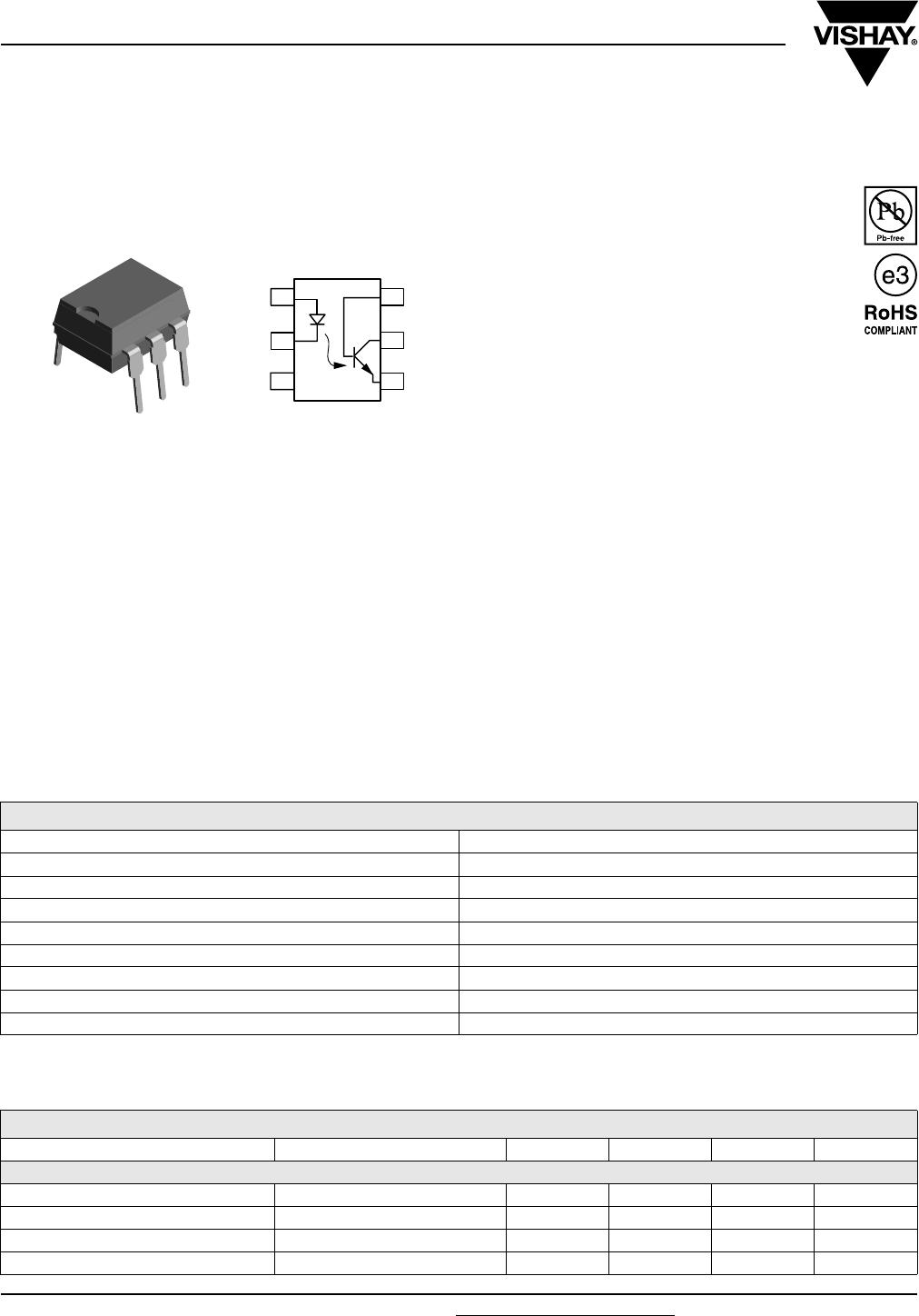
i179004
1
2
3
6
5
4
B
C
E
A
C
NC
ORDER INFORMATION
PART REMARKS
H11D1 CTR > 20 %, DIP-6
H11D2 CTR > 20 %, DIP-6
H11D3 CTR > 20 %, DIP-6
H11D4 CTR > 20 %, DIP-6
H11D1-X007 CTR > 20 %, SMD-6 (option 7)
H11D1-X009 CTR > 20 %, SMD-6 (option 9)
H11D2-X007 CTR > 20 %, SMD-6 (option 7)
H11D3-X007 CTR > 20 %, SMD-6 (option 7)
ABSOLUTE MAXIMUM RATINGS
PARAMETER TEST CONDITION PART SYMBOL VALUE UNIT
INPUT
Reverse voltage V
R
6V
DC forward current I
F
60 mA
Surge forward current t 10 µs I
FSM
2.5 A
Power dissipation P
diss
100 mW
Document Number: 83611 For technical questions, contact: optocoupler.answers@vishay.com
www.vishay.com
Rev. 1.6, 10-Dec-08 289
H11D1, H11D2, H11D3, H11D4
Optocoupler, Phototransistor
Output, with Base Connection,
High BV
CER
Voltage
Vishay Semiconductors
Note
T
amb
= 25 °C, unless otherwise specified.
Stresses in excess of the absolute maximum ratings can cause permanent damage to the device. Functional operation of the device is not implied
at these or any other conditions in excess of those given in the operational sections of this document. Exposure to absolute maximum ratings for
extended periods of the time can adversely affect reliability.
OUTPUT
Collector emitter voltage
H11D1 V
CE
300 V
H11D2 V
CE
300 V
H11D3 V
CE
200 V
H11D4 V
CE
200 V
Collector base voltage
H11D1 V
CBO
300 V
H11D2 V
CBO
300 V
H11D3 V
CBO
200 V
H11D4 V
CBO
200 V
Emitter base voltage V
BEO
7V
Collector current I
C
100 mA
Power dissipation P
diss
300 mW
COUPLER
Isolation test voltage
between emitter and detector
V
ISO
5300 V
RMS
Insulation thickness between emitter
and detector
0.4 mm
Creepage distance 7mm
Clearance distance 7mm
Comparative tracking index per DIN IEC 112/VDE 0303, part 1 175
Isolation resistance
V
IO
= 500 V, T
amb
= 25 °C R
IO
10
12
Ω
V
IO
= 500 V, T
amb
= 100 °C R
IO
10
11
Ω
Storage temperature range T
stg
- 55 to + 150 °C
Operating temperature range T
amb
- 55 to + 100 °C
Junction temperature T
j
100 °C
Soldering temperature
max. 10 s, dip soldering: distance
to seating plane 1.5 mm
T
sld
260 °C
ELECTRICAL CHARACTERISTCS
PARAMETER TEST CONDITION PART SYMBOL MIN. TYP. MAX. UNIT
INPUT
Forward voltage I
F
= 10 mA V
F
1.1 1.5 V
Reverse voltage I
R
= 10 µA V
R
6V
Reverse current V
R
= 6 V I
R
0.01 10 µA
Capacitance V
R
= 0 V, f = 1 MHz C
O
25 pF
Thermal resistance R
thJA
750 K/W
ABSOLUTE MAXIMUM RATINGS
PARAMETER TEST CONDITION PART SYMBOL VALUE UNIT
www.vishay.com For technical questions, contact: optocoupler.answers@vishay.com
Document Number: 83611
290 Rev. 1.6, 10-Dec-08
H11D1, H11D2, H11D3, H11D4
Vishay Semiconductors
Optocoupler, Phototransistor
Output, with Base Connection,
High BV
CER
Voltage
Note
T
amb
= 25 °C, unless otherwise specified.
Minimum and maximum values were tested requierements. Typical values are characteristics of the device and are the result of engineering
evaluations. Typical values are for information only and are not part of the testing requirements.
Note
Switching times measurement-test circuit and waveforms
OUTPUT
Collector emitter breakdown voltage I
CE
= 1 mA, R
BE
= 1 MΩ
H11D1 BV
CER
300 V
H11D2 BV
CER
300 V
H11D3 BV
CER
200 V
H11D4 BV
CER
200 V
Emitter base breakdown voltage I
EB
= 100 µA BV
EBO
7V
Collector emitter capacitance V
CE
= 10 V, f = 1 MHz C
CE
7pF
Collector base capacitance V
CB
= 10 V, f = 1 MHz C
CB
8pF
Emitter base capacitance V
EB
= 5 V, f = 1 MHz C
EB
38 pF
Thermal resistance R
th
250 K/W
COUPLER
Coupling capacitance C
C
0.6 pF
Current transfer ratio
I
F
= 10 mA, V
CE
= 10 V,
R
BE
= 1 MΩ
I
C
/I
F
20 %
Collector emitter,
saturation voltage
I
F
= 10 mA, I
C
= 0.5 mA,
R
BE
= 1 MΩ
V
CEsat
0.25 0.4 V
Collector emitter, leakage current
V
CE
= 200 V, R
BE
= 1 MΩ
H11D1 I
CER
100 nA
H11D2 I
CER
100 nA
V
CE
= 300 V, R
BE
= 1 MΩ,
T
amb
= 100 °C
H11D1 I
CER
250 µA
H11D2 I
CER
250 µA
CURRENT TRANSFER RATIO
PARAMETER TEST CONDITION PART SYMBOL MIN. TYP. MAX. UNIT
Current transfer ratio
I
F
= 10 mA, V
CE
= 10 V,
R
BE
= 1 MΩ
CTR 20 %
SWITCHING CHARACTERISTICS
PARAMETER TEST CONDITION SYMBOL MIN. TYP. MAX. UNIT
Turn-on time
I
C
= 2 mA (to be adjusted by varying I
F
),
R
L
= 100 Ω, V
CC
= 10 V
t
on
s
Rise time
I
C
= 2 mA (to be adjusted by varying I
F
),
R
L
= 100 Ω, V
CC
= 10 V
t
r
2.5 µs
Turn-off time
I
C
= 2 mA (to be adjusted by varying I
F
),
R
L
= 100 Ω, V
CC
= 10 V
t
off
s
Fall time
I
C
= 2 mA (to be adjusted by varying I
F
),
R
L
= 100 Ω, V
CC
= 10 V
t
f
5.5 µs
ELECTRICAL CHARACTERISTCS
PARAMETER TEST CONDITION PART SYMBOL MIN. TYP. MAX. UNIT

H11D1-X009T

Mfr. #:
Manufacturer:
Vishay Semiconductors
Description:
Transistor Output Optocouplers Phototransistor Out Single CTR > 20%
Lifecycle:
New from this manufacturer.
Delivery:
DHL FedEx Ups TNT EMS
Payment:
T/T Paypal Visa MoneyGram Western Union