Expand menu
Hello, Sign in
My Account
0
Cart
Home
Products
Sensors
Semiconductors
Passive Components
Connectors
Power
Electromechanical
Optoelectronics
Circuit Protection
Integrated Circuits - ICs
Main Products
Manufacturers
Blog
Services
About OMO
About Us
Contact Us
Check Stock
ZL40204LDG1
P1-P3
P4-P6
P7-P9
P10-P12
P13-P15
P16-P18
P19-P21
P22-P24
P25-P26
ZL40204
Data Sheet
4
Microsemi Corporation
Change Summary
Page
Item
Change
7
7
13
Figure 4
Figure 5
Figure 16
Changed text to indicate the circuit is not reco
mmended for
VDD_dr
iver=2.5V
.
Changed pull-up and pull-
down resistors from 2kOhm to
10
0Ohm.
Corrected typo: changed R values fr
om 143 and 82 to 120
an
d 60 to ma
tch othe
r fanout
buffer data sheets.
Below are the changes from the November 201
2 issue to the February 2013 issue:
ZL40204
Data Sheet
5
Microsemi Corporation
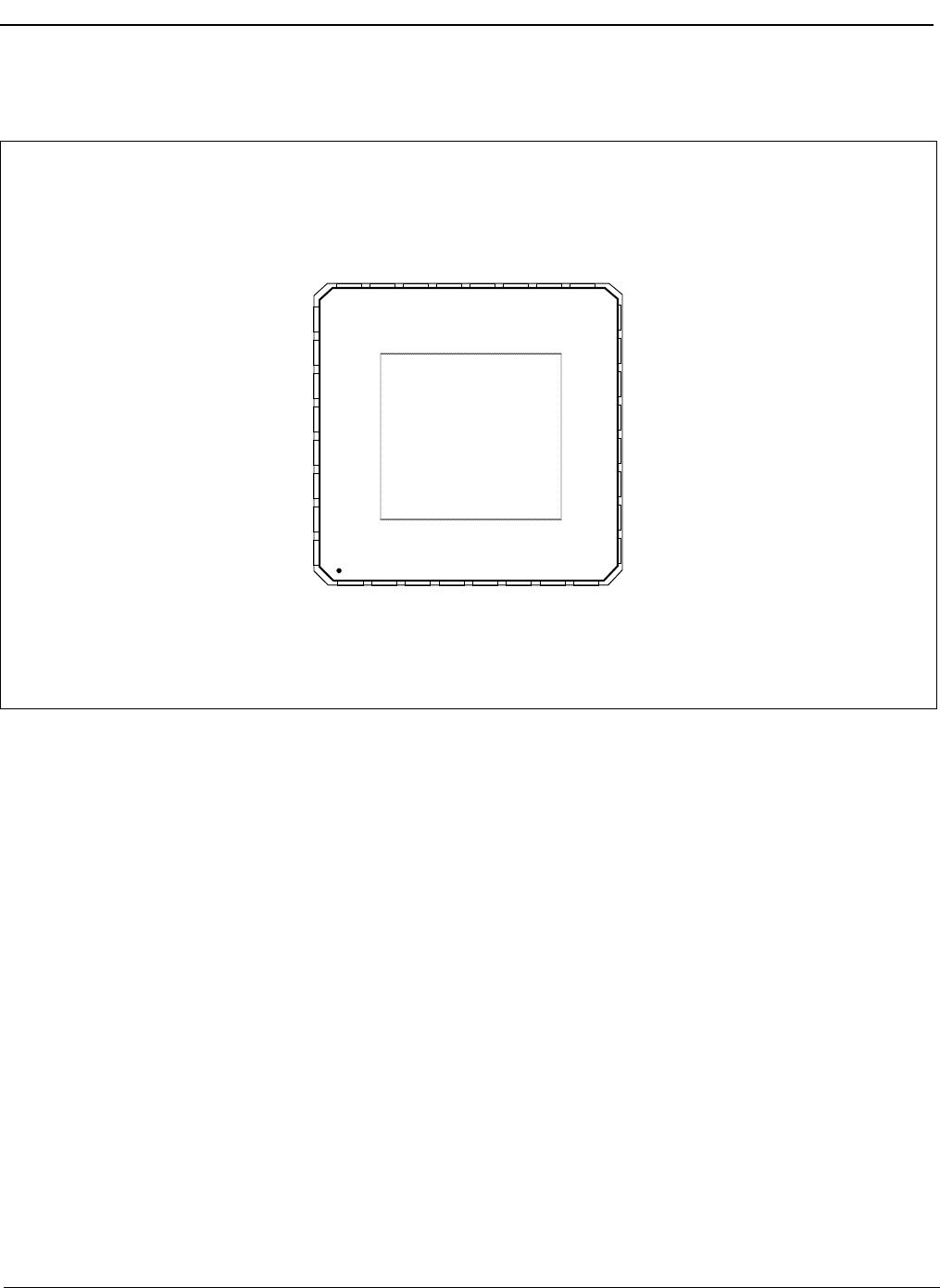
1.0 Package Description
The device is pa
ckaged in a 32 pin QFN
26
28
30
32
12
10
8
6
4
2
NC
out5_p
out4_n
out5_n
NC
gnd
clk_p
VDD_core
out1_n
NC
out0_n
out1_p
gnd
out3_n
vdd
gnd
out2_p
14
16
18
22
24
20
vdd
NC
out0_p
NC
clk_n
out2_n
gnd
out3_p
vdd
NC
NC
VDD_core
out4_p
vdd
vt
gnd (E-p
ad)
NC
Figure 2 - Pin Connections
ZL40204
Data Sheet
6
Microsemi Corporation
2.0 Pin Description
Pin #
Name
Description
3, 6
clk_p, clk_
n,
Differential Input (Analog Input).
Differential (or singled en
ded
) input signals. For all
input signal configuration
s, s
ee “Clock Inputs” on p
age 6
28, 27,
26, 25,
24, 23,
18, 17,
16, 15,
14, 13
out0_p, out0_n
out1_p, out1_n
out2_p, out2_n
out3_p, out3_n
out4_p, out4_n
out5_p, out5_n
Differential Outpu
t (Analog Output).
Dif
ferential outputs.
9, 19,
22, 32
vdd
Positive Supply V
oltage.
2.5 V
DC
or 3.3 V
DC
nominal.
1, 8
vdd_core
Positive Supply V
oltage.
2.5 V
DC
or 3.3 V
DC
nominal.
2, 7,
20, 21
gnd
Ground.
0 V
.
4, 5
10, 1
1,
12, 29,
30, 31
NC
No Connection.
L
eave unconnected.
P1-P3
P4-P6
P7-P9
P10-P12
P13-P15
P16-P18
P19-P21
P22-P24
P25-P26
ZL40204LDG1
Mfr. #:
Buy ZL40204LDG1
Manufacturer:
Microchip / Microsemi
Description:
Clock Buffer 1:6 LVPECL Fanout Buffer w/Ext. Term.
Lifecycle:
New from this manufacturer.
Delivery:
DHL
FedEx
Ups
TNT
EMS
Payment:
T/T
Paypal
Visa
MoneyGram
Western
Union
Products related to this Datasheet
ZL40204LDG1
ZL40204LDF1