14
IDT72V801/72V8211/72V821/72V831/72V841/72V851 3.3V DUAL CMOS SyncFIFO
TM
DUAL 256 x 9, DUAL 512 x 9, DUAL 1K x 9, DUAL 2K x 9, DUAL 4K x 9, DUAL 8K x 9
COMMERCIAL AND INDUSTRIAL
TEMPERATURE RANGES
OPERATING CONFIGURATIONS
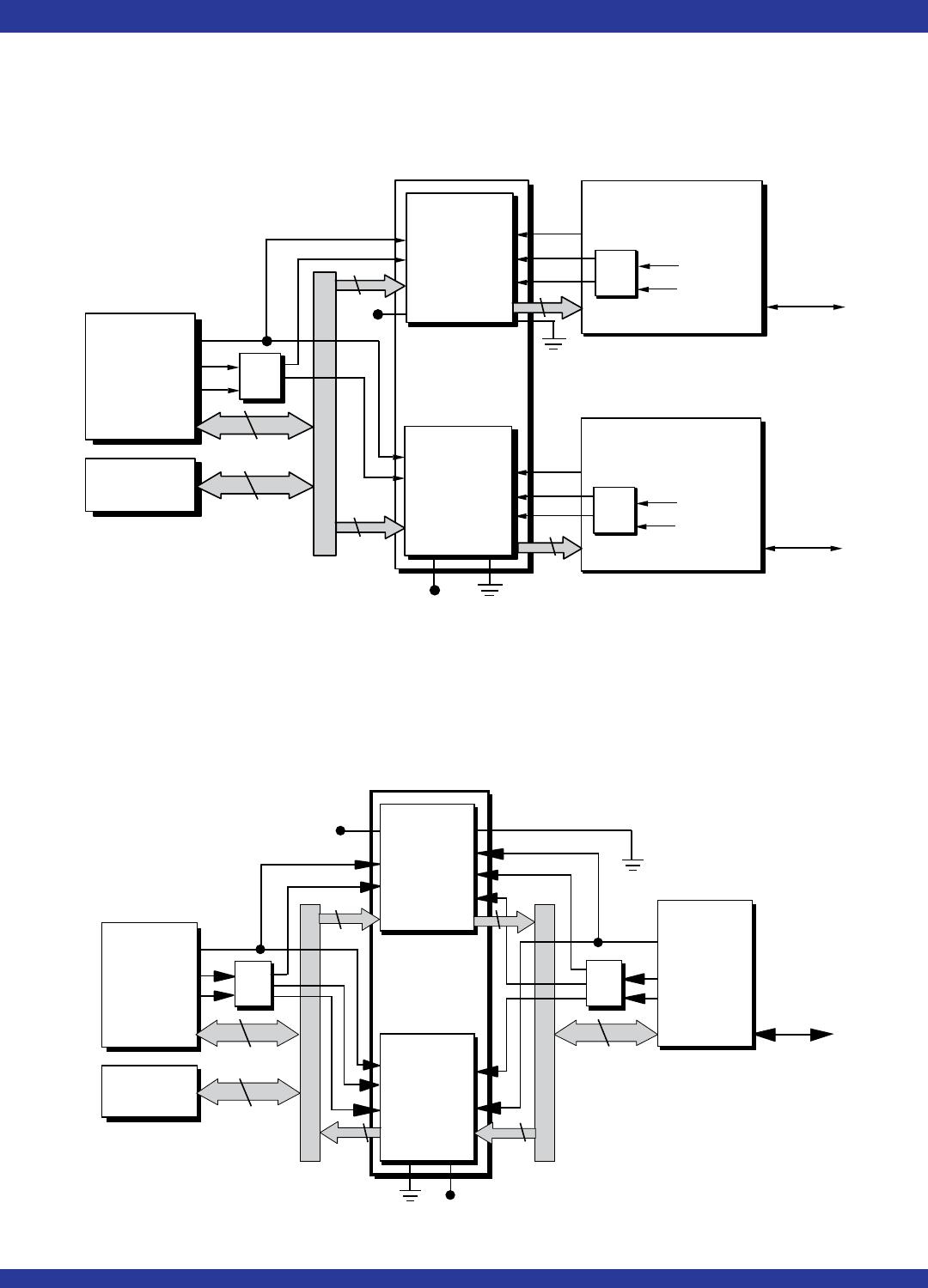
SINGLE DEVICE CONFIGURATION — When FIFO A (B) is in a Single
Device Configuration, the Read Enable 2 RENA2 ( RENB2) control input can
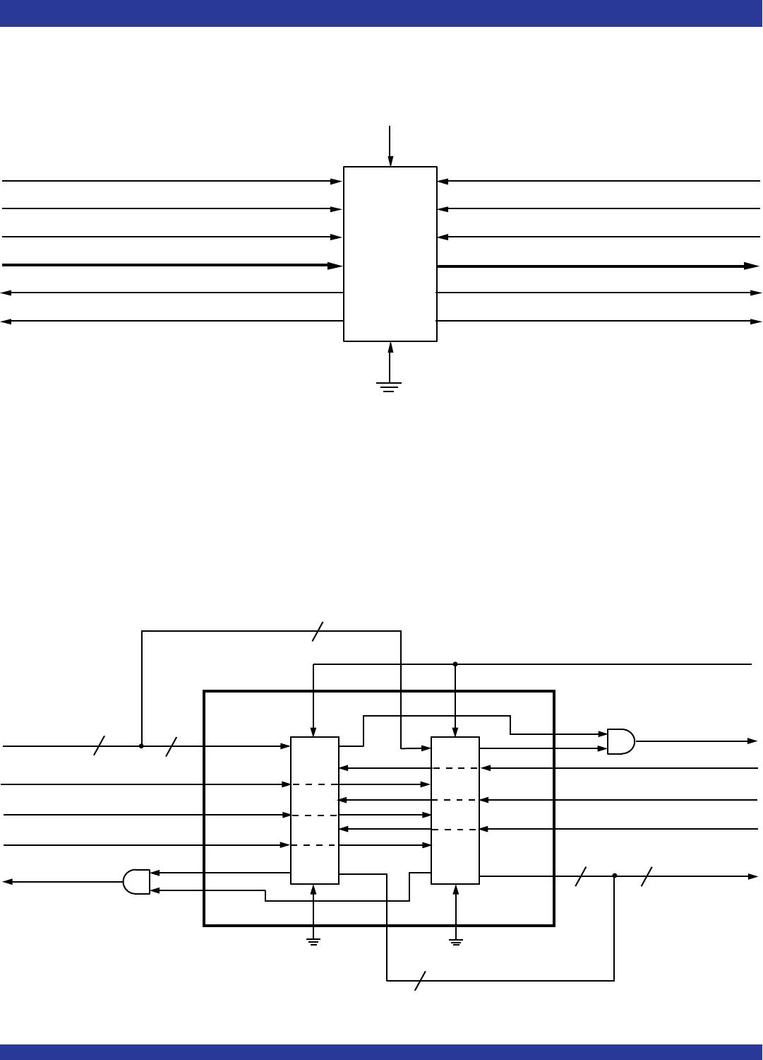
Figure 15. Block diagram of the two FIFOs contained in one IDT72V801/72V811/72V821/72V831/72V841/72V851
configured for an 18-bit width-expansion
be grounded (see Figure 14). In this configuration, the Write Enable 2/Load
WENA2/LDA (WENB2/LDB) pin is set LOW at Reset so that the pin operates
as a control to load and read the programmable flag offsets.
Figure 14. Block Diagram of One of the IDT72V801/72V811/72V821/72V831/72V841/72V851's
two FIFOs configured as a single device
WIDTH EXPANSION CONFIGURATION — Word width may be in-
creased simply by connecting the corresponding input control signals of
FIFOs A and B. A composite flag should be created for each of the end-
point status flags EFA and EFB, also FFA and FFB). The partial status flags PAEA,
PAFB, PAEA and PAFB can be detected from any one device. Figure 15
demonstrates an 18-bit word width using the two FIFOs contained in one
IDT72V801/72V811/72V821/72V831/72V841/72V851. Any word width can
be attained by adding additional IDT72V801/72V811/72V821/72V831/
72V841/72V851s.
When these devices are in a Width Expansion Configuration, the Read
Enable 2 (RENA2 and RENB2) control inputs can be grounded (see Figure
15). In this configuration, the Write Enable 2/Load (WENA2/LDA, WENB2/LDB)
pins are set LOW at Reset so that the pin operates as a control to load and read
the programmable flag offsets.
QA
0
- QA
8
(QB
0
- QB
8
)
DA
0
- DA
8
(DB
0
- DB
8
)
RSA (RSB)
RCLKA (RCLKB)
RENA1 (RENB1)
OEA (OEB)
EFA (EFB)
PAEA (PAEB)
RENA2 (RENB2)
WCLKA (WCLKB)
WENA1 (WENB1)
WENA2/LDA (WENB2/LDB)
FFA (FFB)
PAFA (PAFB)
IDT
72V801
72V811
72V821
72V831
72V841
72V851
FIFO
A (B)
4093 drw 16
DATA IN
WRITE CLOCK
18
9
RSB
READ CLOCK
9
18
RENB2RENA2
WRITE ENABLE
FFA
EFB
OUTPUT ENABLE
READ ENABLE
9
WRITE ENABLE/LOAD
FFB
EFA
RSA
RAM
ARRAY
A
DATA OUT
RCLKA
EMPTY FLAG
RENB1
RENA1
OEB
OEA1
RCLKB
WCLKA
WCLKB
WENA1
WENB1
DA0 - DA8
DB0 - DB8
QA0 - QA8
QB0 - QB8
WENA2/LDA
2WENB2/LDB
RESET
9
FULL FLAG
4093 drw 17
RAM
ARRAY
B
256x9
512x9
1,024x9
2,048x9
4,096x9
8,192x9
256x9
512x9
1,024x9
2,048x9
4,096x9
8,192x9