12
IDT72V801/72V8211/72V821/72V831/72V841/72V851 3.3V DUAL CMOS SyncFIFO
TM
DUAL 256 x 9, DUAL 512 x 9, DUAL 1K x 9, DUAL 2K x 9, DUAL 4K x 9, DUAL 8K x 9
COMMERCIAL AND INDUSTRIAL
TEMPERATURE RANGES
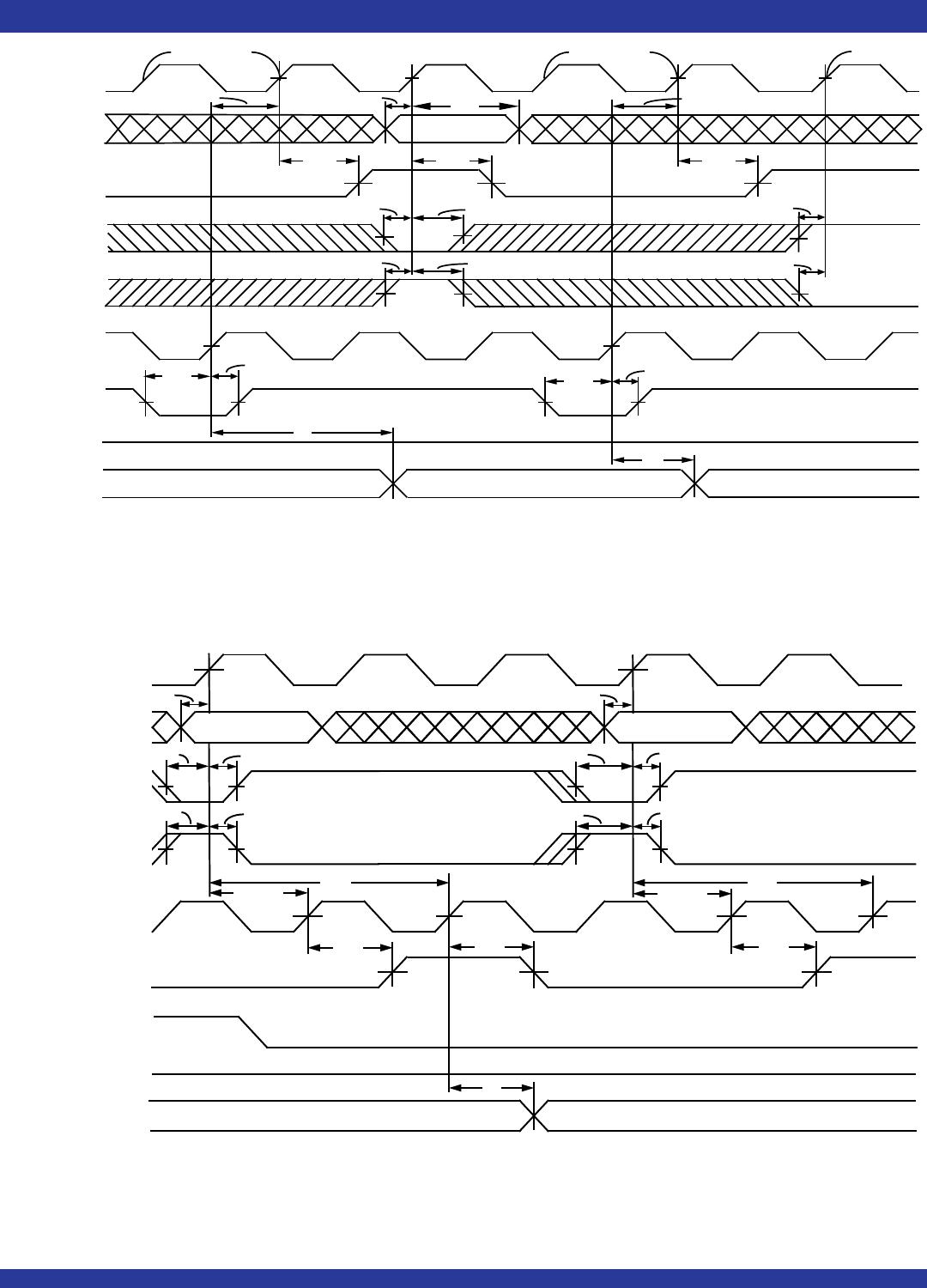
NOTES:
1. m = PAF offset.
2. (256-m) words for the IDT72V801, (512-m) words the IDT72V811, (1,024-m) words for the IDT72V821, (2,048-m) words for the IDT72V831, (4,096-m) words for the IDT72V841,
or (8,192-m) words for the IDT72V851.
3. tSKEW2 is the minimum time between a rising RCLKA (RCLKB) edge and a rising WCLKA (WCLKB) edge for PAFA (PAFB) to change during that clock cycle. If the time between
the rising edge of RCLKA (RCLKB) and the rising edge of WCLKA (WCLKB) is less than tSKEW2, then PAFA (PAFB) may not change state until the next WCLKA (WCLKB)
rising edge.
4. If a write is performed on this rising edge of the Write Clock, there will be Full - (m-1) words in FIFO A (B) when PAFA (PAFB) goes LOW.
Figure 10. Programmable Full Flag Timing
Figure 11. Programmable Empty Flag Timing
NOTES:
1. n = PAE offset.
2. tSKEW2 is the minimum time between a rising WCLKA (WCLKB) edge and a rising RCLKA (RCLKB) edge for PAEA (PAEB) to change during that clock cycle. If the time between
the rising edge of WCLKA (WCLKB) and the rising edge of RCLKA (RCLKB) is less than tSKEW2, then PAEA (PAEB) may not change state until the next RCLKA (RCLKB)
rising edge.
3. If a read is performed on this rising edge of the Read Clock, there will be Empty + (n-1) words in FIFO A (B) when PAEA (PAEB) goes LOW.
t
ENS
t
ENH
t
ENS
t
ENH
t
ENS
t
ENH
WCLKA
(WCLKB)
WENA1
(WENB1
WENA2
(WENB2)
(If Applicable)
PAFA
(PAFB)
RCLKA
(RCLKB)
RENA1, RENA2
(RENB1, RENB2)
(4)
t
PAF
(1)
Full - (m+1) words in FIFO
Full - m words in FIFO
(2)
t
CLKH
t
CLKL
t
SKEW2
(3)
t
PAF
4093 drw 12
WCLKA
(WCLKB)
WENA1
(WENB1)
WENA2
(WENB2)
(If Applicable)
PAEA,
PAEB
RCLKA
(RCLKB)
RENA1, RENA2
(RENB1, RENB2)
t
ENS
t
ENH
t
ENS
t
ENH
t
SKEW2
(2)
t
ENS
t
ENH
t
PAE
t
PAE
(3)
(1)
n words in FIFO
n+1 words in FIFO
t
CLKH
t
CLKL
4093 drw 13