QUICK START GUIDE FOR DEMONSTRATION CIRCUIT 559
SYNCHRONOUS BOOST CONVERTER WITH OUTPUT DISCONNECT
1
LTC3429
DESCRIPTION
Demonstration circuit 559 is a high efficiency synchro-
nous boost DC/DC converter with output disconnect,
inrush current limiting and soft-start functions featuring
the LTC3429. The board is capable of supplying 90mA
from a single AA cell input or 250mA from a 2-cell input
with a 3.3V output. The input range is from 1V to 3.3V.
DC559 version A uses the LTC3429; version B uses the
LTC3429B. The LTC3429 shifts automatically to power
saving Burst Mode operation at light loads; whereas the
LTC3429B operates at a fixed frequency for all loads with
minimum output voltage ripple.
A switching frequency of 500KHz allows up to 95% effi-
ciency with a tiny solution footprint. Typical applications
include MP3 players, GPS receivers, digital cameras,
PDAs, LCD bias supplies and wireless handsets.
Design files for this circuit board are available. Call
the LTC factory.
Table 1.
Performance Summary
PARAMETER CONDITION VALUE
Maximum Load Current, Min Vout = 3.3V, Vin = 1.0V 90mA
Maximum Load Current, Min Vout = 3.3V, Vin = 2.0V 250mA
Switching Frequency, Typ 500KHz
Efficiency, Typ Vout = 3.3V, Vin = 2.8V, Iout = 100mA 95%
Output Ripple, Typ Vout = 3.3V, V
IN
= 1.5V, I
OUT
= 100mA (20MHz BW) 20mV
P–P
QUICK START PROCEDURE
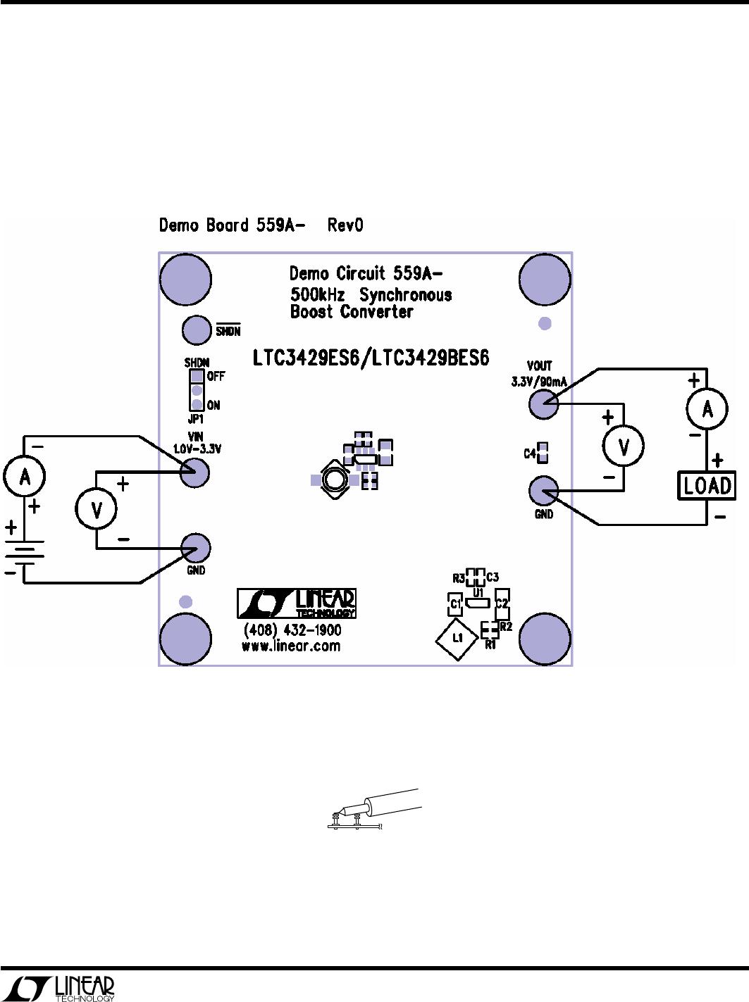
Demonstration circuit 559 is easy to set up to evaluate
the performance of the LTC3429. Refer to Figure 1 for
proper measurement equipment setup and follow the
procedure below:
NOTE:
When measuring the input or output voltage rip-
ple, care must be taken to avoid a long ground lead on
the oscilloscope probe. Measure the input or output
voltage ripple by touching the probe tip directly across
the Vin or Vout and GND terminals. See Figure 2 for
proper scope probe technique.
1.
Place the jumper in the following position:
On
2.
With power off, connect the input power supply to Vin
and GND. Connect the load to Vout and GND. Set ini-
tial load = 0A (no load).
3.
Turn on the power at the input.
NOTE:
Make sure that the input voltage does not ex-
ceed 4.4V.