NB3N3002DTR2G

NB3N3002
www.onsemi.com
4
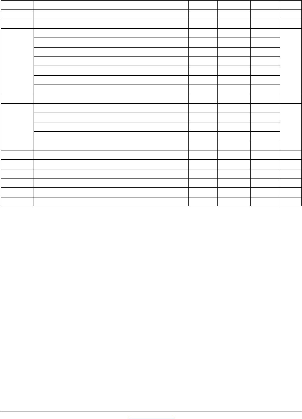
Table 6. AC CHARACTERISTICS (V
DD
= 3.3 V ±5%, GND = 0 V, T
A
= −40°C to +85°C; Note 7)
Symbol
Characteristic Min Typ Max Unit
f
CLKIN
Clock/Crystal Input Frequency 25 MHz
f
CLKOUT
Output Clock Frequency 25 200 MHz
q
NOISE
Phase−Noise Performance f
CLK
= 200 MHz/100 MHz
dBc/Hz
@ 100 Hz offset from carrier −103/−109
@ 1 kHz offset from carrier −118/−127.8
@ 10 kHz offset from carrier −122/−136.2
@ 100 kHz offset from carrier −130/−138.8
@ 1 MHz offset from carrier −138/−138.2
@ 10 MHz offset from carrier −149/−164
t
jit(
f
)
RMS Phase Jitter (at 125 MHz @ 1 MHz − 40 MHz) 0.25 0.50 ps
t
jitter
(TIE)
TIE RMS Jitter (Note 8) f
CLK
= 200 MHz 2.5
ps
Cycle−to−Cycle RMS Jitter (Note 9) f
CLK
= 200 MHz 2 5
Cycle−to−Cycle Peak to Peak Jitter (Note 9) f
CLK
= 200 MHz 20 35
Period RMS Jitter (Note 9) f
CLK
= 200 MHz 1.5 3
Period Peak−to−Peak Jitter (Note 9) f
CLK
= 200 MHz 10 20
OE Output Enable/Disable Time 1.0
ms
t
DUTY_CYCLE
Output Clock Duty Cycle (Measured at cross point) 45 50 55 %
t
R
Output Risetime (Measured from 175 mV to 525 mV, Figure 4) 175 340 700 ps
t
F
Output Falltime (Measured from 525 mV to 175 mV, Figure 4) 175 340 700 ps
Dt
R
Output Risetime Variation (Single−Ended) 125 ps
Dt
F
Output Falltime Variation (Single−Ended) 125 ps
NOTE: Device will meet the specifications after thermal equilibrium has been established when mounted in a test socket or printed circuit
board with maintained transverse airflow greater than 500 lfpm.
6. NB3N circuits are designed to meet the DC specifications shown in the above table after thermal equilibrium has been established. The circuit
is in a test socket or mounted on a printed circuit board and transverse airflow greater than 500 lfpm is maintained.
7. Measurement taken from differential output on single−ended channel terminated with R
S
= 33.2 W, R
L
= 49.9 W, with load capacitance of
2 pF and current biasing resistor, R
REF
, from I
REF
(Pin 9) to GND of 475 W. See Figures 3 and 4.
8. Sampled with 20000 cycles to capture jitter component down to 100 kHz.
9. Sampled with 20000 cycles.
NB3N3002
www.onsemi.com
5
Table 7. AC ELECTRICAL CHARACTERISTICS − PCI EXPRESS JITTER SPECIFICATIONS,
V
DD
= 3.3 V ± 5%, T
A
= −40°C to 85°C
Symbol
Parameter Conditions (Notes 10 and 11) Min Typ Max
Industry
Limit
Unit
t
jphPCIeG1
RMS Phase Jitter
PCIe Gen 1 (Notes 12 and 13) 10 16 86 ps (p−p)
t
jphPCIeG2
PCIe Gen 2 Lo Band
10 kHz < f < 1.5 MHz (Note 12)
0.2 0.25 3
ps
(rms)
PCIe Gen 2 High Band
1.5 MHz < f < Nyquist (50 MHz)
(Note 12)
0.9 1.2 3.1
ps
(rms)
t
jphPCIeG3
PCIe Gen 3
(PLL BW of 2−4 MHz, CDR = 10 MHz)
(Note 12)
0.2 0.3 1
ps
(rms)
t
jphPCIeG4
PCIe Gen 4
(PLL BW of 2−4 MHz, CDR = 10 MHz)
(Note 12)
0.21 0.3 0.5
ps
(rms)
t
jphUPI
UPI
(9.6 Gb/s, 10.4 Gb/s or 11.2 Gb/s, 100 MHz, 12 UI)
0.62 0.7 1.0
ps
(rms)
t
jphQPI_SMI
QPI & SMI
(100.00 MHz or 133.33 MHz,
4.8 Gb/s, 6.4 Gb/s 12UI) (Note 14)
0.1 0.3 0.5
ps
(rms)
QPI & SMI
(100.00 MHz, 8.0 Gb/s, 12UI) (Note 14)
0.1 0.15 0.3
ps
(rms)
QPI & SMI
(100.00 MHz, 9.6 Gb/s, 12UI) (Note 14)
0.07 0.1 0.2
ps
(rms)
Product parametric performance is indicated in the Electrical Characteristics for the listed test conditions, unless otherwise noted. Product
performance may not be indicated by the Electrical Characteristics if operated under different conditions.
10.Applies to all outputs.
11. Guaranteed by design and characterization, not tested in production
12.See http://www.pcisig.com for complete specs
13.Sample size of at least 100K cycles. This figures extrapolates to 108 ps pk−pk @ 1M cycles for a BER of 1−12.
14.Calculated from Intel−supplied Clock Jitter Tool v 1.6.3.
Figure 3. Typical Termination for Output Driver and Device Evaluation
Z
o
= 50 W
Z
o
= 50 W
R
L
= 49.9 W
R
L
=
49.9 W
R
L
= 33.2 W
R
L
= 33.2 W
HCSL
Driver
HCSL
Receiver
R
REF
= 475 W
I
REF
NB3N3002
www.onsemi.com
6
Figure 4. HCSL Output Parameter Characteristics
t
R
t
F
525 mV
175 mV
525 mV
175 mV
340 ps
340 ps
700 mV
0 mV
Figure 5. HCSL Interface Termination to LVDS
Z
o
= 50 W
Z
o
= 50 W
R
L
= 150 W R
L
= 150 W
HCSL
Driver
LVDS
Receiver
Qx
Qx
100 W 100 W
IREF
R
REF
= 475 W
ORDERING INFORMATION
Device Package Shipping
NB3N3002DTG TSSOP−16
(Pb−Free)
96 Units / Rail
NB3N3002DTR2G TSSOP−16
(Pb−Free)
2500 / Tape & Reel
For information on tape and reel specifications, including part orientation and tape sizes, please refer to our Tape and Reel Packaging
Specifications Brochure, BRD8011/D.

NB3N3002DTR2G

Mfr. #:
Manufacturer:
ON Semiconductor
Description:
Phase Locked Loops - PLL CLK GEN LVPECL DIFF OUT
Lifecycle:
New from this manufacturer.
Delivery:
DHL FedEx Ups TNT EMS
Payment:
T/T Paypal Visa MoneyGram Western Union

Products related to this Datasheet