© Semiconductor Components Industries, LLC, 2006
September, 2006 − Rev. 6
1 Publication Order Number:
NCP346/D
NCP346
Overvoltage Protection IC
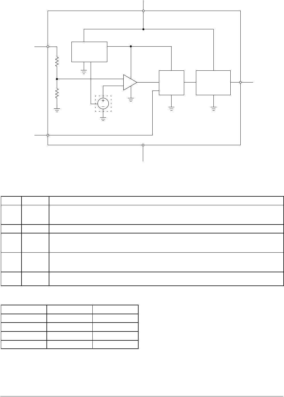
The NCP346 Overvoltage Protection circuit (OVP) protects
sensitive electronic circuitry from overvoltage transients and power
supply faults when used in conjunction with an external P−channel
FET. The device is designed to sense an overvoltage condition and
quickly disconnect the input voltage supply from the load before any
damage can occur. The OVP consists of a precise voltage reference, a
comparator with hysteresis, control logic, and a MOSFET gate driver.
The OVP is designed on a robust BiCMOS process and is intended to
withstand voltage transients up to 30 V.
The device is optimized for applications that have an external
AC/DC adapter or car accessory charger to power the product and/or
recharge the internal batteries. The nominal overvoltage thresholds are
4.45 and 5.5 V and can be adjusted upward with a resistor divider
between the V
CC
, IN, and GND pins. It is suitable for single cell
Li−Ion applications as well as 3/4 cell NiCD/NiMH applications.
Features
Overvoltage Turn−Off Time of Less Than 1.0 msec
Accurate Voltage Threshold of 4.45 V and 5.5 V (Nominal)
CNTRL Input Compatible with 1.8 V Logic Levels
These are Pb−Free Devices
Typical Applications
Cellular Phones
Digital Cameras
Portable Computers and PDAs
Portable CD and other Consumer Electronics
+
OUT
IN
V
ref
GND CNTRL
+
V
CC
Logic
FET
Driver
LOAD
AC/DC Adapter or
Accessory Charger
C1
Schottky
Diode
Microprocessor port
P−CH
Figure 1. Simplified Application Diagram
NCP346
Note: This device contains 89 active transistors
(optional)
(optional)
THIN SOT−23−5
SN SUFFIX
CASE 483
PIN CONNECTIONS &
MARKING DIAGRAM
Device Package Shipping
ORDERING INFORMATION
NCP346SN1T1G
SOT−23−5
(Pb−Free)
3000 / Tape & Ree
l
(7 inch Reel)
xxx = SQZ for NCP346SN1
= SRD for NCP346SN2
A = Asembly Location
Y = Year
W = Work Week
G = Pb−Free Package
(Note: Microdot may be in either location
)
NCP346SN2T1G
1
5
For information on tape and reel specifications,
including part orientation and tape sizes, please
refer to our Tape and Reel Packaging Specification
s
Brochure, BRD8011/D.
http://onsemi.com
1
3
IN
OUT
2
GND
CNTRL
4
V
CC
5
(Top View)
xxxAYWG
G
NCP346
http://onsemi.com
2
Figure 2. Detailed Block Diagram
+
CNTRL
(3)
OUT
(1)
GND
(2)
LOGIC
BLOCK
DRIVER
Pre−regulator
V
CC
(5)
IN
(4)
ON/OFF OUT
V5
R1
R2
COMP
Bandgap
Reference
V
CC
V
CC
PIN FUNCTION DESCRIPTIONS
Pin # Symbol Pin Description
1 OUT This signal drives the gate of a P−channel MOSFET. It is controlled by the voltage level on IN or the logic state of
the CNTRL input. When an overvoltage event is detected, the OUT pin is driven to within 1.0 V of V
CC
in less
than 1.0 msec provided that gate and stray capacitance is less than 12 nF.
2 GND Circuit Ground
3 CNTRL This logic signal is used to control the state of OUT and turn−on/off the P−channel MOSFET. A logic High results
in the OUT signal being driven to within 1.0 V of V
CC
which disconnects the FET. The input is tied Low via an
internal 50 kW pull−down resistor. It is recommended that the input be connected to GND if it is not used.
4 IN This pin senses an external voltage point. If the voltage on this input rises above the overvoltage threshold (V
th
),
the OUT pin will be driven to within 1.0 V of V
CC
, thus disconnecting the FET. The nominal threshold level can be
increased with the addition of an external resistor divider between IN, V
CC
, and GND.
5 V
CC
Positive Voltage supply. OUT is guaranteed to be in low state (MOSFET ON) as long as V
CC
remains above
2.5 V, and below the overvoltage threshold.
TRUTH TABLE
IN CNTRL OUT
<V
th
L GND
<V
th
H V
CC
>V
th
L V
CC
>V
th
H V
CC
NCP346
http://onsemi.com
3
MAXIMUM RATINGS (T
A
= 25°C unless otherwise noted.)
Rating
Pin Symbol Min Max Unit
OUT Voltage to GND 1 V
O
−0.3 30 V
Input and CNTRL Pin Voltage to GND 4
3
V
input
V
CNTRL
−0.3
−0.3
30
13
V
Input Pin Voltage to V
CC
4, 5 V(V
CC,
IN) −0.3 15 V
V
CC
Maximum Range 5 V
CC(max)
−0.3 30 V
Maximum Power Dissipation at T
A
= 85°C P
D
0.216 W
Thermal Resistance, Junction−to−Air
R
q
JA
300 °C/W
Junction Temperature T
J
150 °C
Operating Ambient Temperature T
A
−40 85 °C
V
CNTRL
Operating Voltage 3 0 5.0 V
Storage Temperature Range T
stg
−65 150 °C
Stresses exceeding Maximum Ratings may damage the device. Maximum Ratings are stress ratings only. Functional operation above the
Recommended Operating Conditions is not implied. Extended exposure to stresses above the Recommended Operating Conditions may affect
device reliability.
ATTRIBUTES
Characteristic Value
ESD Protection
Human Body Model (HBM) per JEDEC Standard JESD22−A114
Machine Model (MM) per JEDEC Standard JESD22−A114
v 2.5 kV
v 250 V
Moisture Sensitivity, Indefinite Time Out of Drypack (Note 1) Level 1
Transistor Count 89
Latchup Current Maximum Rating per JEDEC Standard EIA/JESD78 v 150 mA
1. For additional Moisture Sensitivity information, refer to Application Note AND8003/D.

NCP346SN2T1G

Mfr. #:
Manufacturer:
ON Semiconductor
Description:
IC DETECTOR OVER VOLTAGE 5TSOP
Lifecycle:
New from this manufacturer.
Delivery:
DHL FedEx Ups TNT EMS
Payment:
T/T Paypal Visa MoneyGram Western Union

Products related to this Datasheet