SMBJ5.0A thru SMBJ188A
www.vishay.com
Vishay General Semiconductor
Revision: 14-Jul-17
2
Document Number: 88392
For technical questions within your region: DiodesAmericas@vishay.com
, DiodesAsia@vishay.com, DiodesEurope@vishay.com
THIS DOCUMENT IS SUBJECT TO CHANGE WITHOUT NOTICE. THE PRODUCTS DESCRIBED HEREIN AND THIS DOCUMENT
ARE SUBJECT TO SPECIFIC DISCLAIMERS, SET FORTH AT www.vishay.com/doc?91000
Notes
(1)
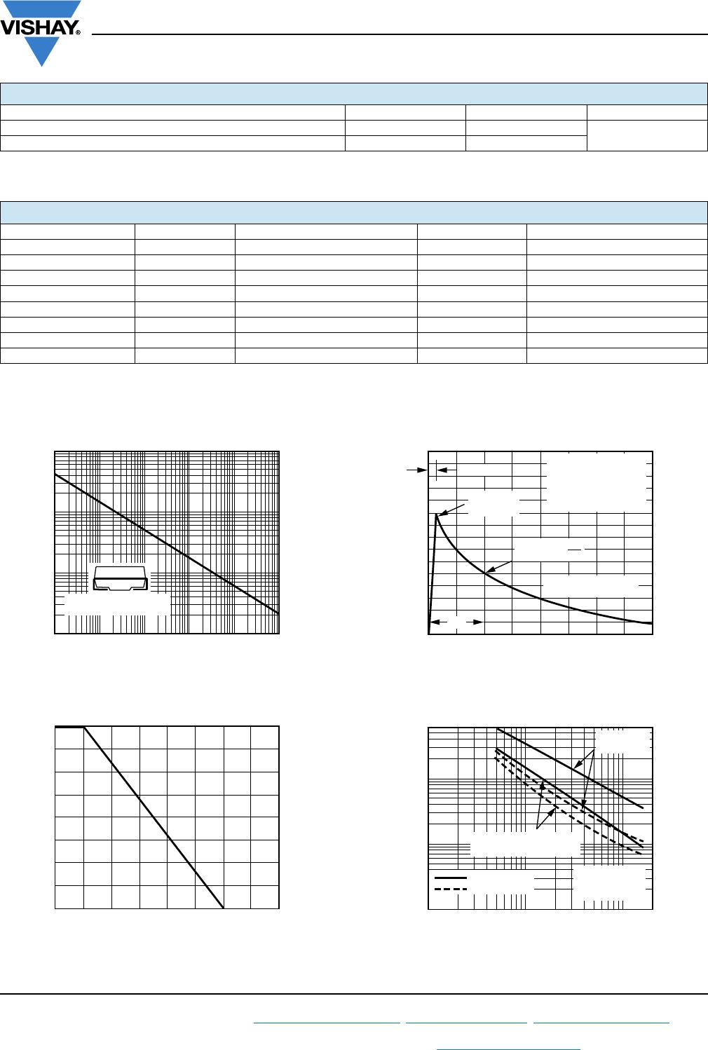
Pulse test: t
p
≤ 50 ms
(2)
Surge current waveform per fig. 3 and derate per fig. 2
(3)
For bi-directional types having V
WM
of 10 V and less, the I
D
limit is doubled
(4)
All terms and symbols are consistent with ANSI/IEEE C62.35
(5)
For the bi-directional SMBJ5.0CA, the maximum V
BR
is 7.25 V
(6)
V
F
= 3.5 V max. at I
F
= 50 A (uni-directional only)
(+)
Underwriters laboratory recognition for the classification of protectors (QVGQ2) under the UL standard for safety 497B and file number
E136766 for both uni-directional and bi-directional devices
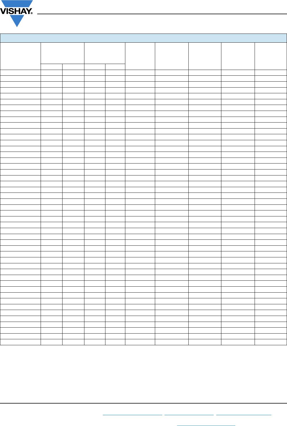
ELECTRICAL CHARACTERISTICS (T
A
= 25 °C unless otherwise noted)
DEVICE TYPE
MODIFIED
“J” BEND LEAD
DEVICE MARKING
CODE
BREAKDOWN
VOLTAGE
V
BR
AT I
T
(1)
(V)
TEST
CURRENT
I
T
(mA)
STAND-OFF
VOLTAGE
V
WM
(V)
MAXIMUM
REVERSE
LEAKAGE
AT V
WM
I
D
(μA)
(3)
MAXIMUM
PEAK PULSE
SURGE
CURRENT
I
PPM
(A)
(2)
MAXIMUM
CLAMPING
VOLTAGE AT
I
PPM
V
C
(V)
UNI BI MIN. MAX.
(+)
SMBJ5.0A
(5)
KE KE 6.40 7.07 10 5.0 800 65.2 9.2
(+)
SMBJ6.0A KG KG 6.67 7.37 10 6.0 800 58.3 10.3
(+)
SMBJ6.5A KK AK 7.22 7.98 10 6.5 500 53.6 11.2
(+)
SMBJ7.0A KM KM 7.78 8.60 10 7.0 200 50.0 12.0
(+)
SMBJ7.5A KP AP 8.33 9.21 1.0 7.5 100 46.5 12.9
(+)
SMBJ8.0A KR AR 8.89 9.83 1.0 8.0 50 44.1 13.6
(+)
SMBJ8.5A KT AT 9.44 10.4 1.0 8.5 20 41.7 14.4
(+)
SMBJ9.0A KV AV 10.0 11.1 1.0 9.0 10 39.0 15.4
(+)
SMBJ10A KX AX 11.1 12.3 1.0 10 5.0 35.3 17.0
(+)
SMBJ11A KZ KZ 12.2 13.5 1.0 11 5.0 33.0 18.2
(+)
SMBJ12A LE BE 13.3 14.7 1.0 12 5.0 30.2 19.9
(+)
SMBJ13A LG LG 14.4 15.9 1.0 13 1.0 27.9 21.5
(+)
SMBJ14A LK BK 15.6 17.2 1.0 14 1.0 25.9 23.2
(+)
SMBJ15A LM BM 16.7 18.5 1.0 15 1.0 24.6 24.4
(+)
SMBJ16A LP LM 17.8 19.7 1.0 16 1.0 23.1 26.0
(+)
SMBJ17A LR LR 18.9 20.9 1.0 17 1.0 21.7 27.6
(+)
SMBJ18A LT BT 20.0 22.1 1.0 18 1.0 20.5 29.2
(+)
SMBJ20A LV LV 22.2 24.5 1.0 20 1.0 18.5 32.4
(+)
SMBJ22A LX BX 24.4 26.9 1.0 22 1.0 16.9 35.5
(+)
SMBJ24A LZ BZ 26.7 29.5 1.0 24 1.0 15.4 38.9
(+)
SMBJ26A ME CE 28.9 31.9 1.0 26 1.0 14.3 42.1
(+)
SMBJ28A MG MG 31.1 34.4 1.0 28 1.0 13.2 45.4
(+)
SMBJ30A MK CK 33.3 36.8 1.0 30 1.0 12.4 48.4
(+)
SMBJ33A MM CM 36.7 40.6 1.0 33 1.0 11.3 53.3
(+)
SMBJ36A MP CP 40.0 44.2 1.0 36 1.0 10.3 58.1
(+)
SMBJ40A MR CR 44.4 49.1 1.0 40 1.0 9.3 64.5
(+)
SMBJ43A MT CT 47.8 52.8 1.0 43 1.0 8.6 69.4
(+)
SMBJ45A MV MV 50.0 55.3 1.0 45 1.0 8.3 72.7
(+)
SMBJ48A MX MX 53.3 58.9 1.0 48 1.0 7.8 77.4
(+)
SMBJ51A MZ MZ 56.7 62.7 1.0 51 1.0 7.3 82.4
(+)
SMBJ54A NE NE 60.0 66.3 1.0 54 1.0 6.9 87.1
(+)
SMBJ58A NG NG 64.4 71.2 1.0 58 1.0 6.4 93.6
(+)
SMBJ60A NK NK 66.7 73.7 1.0 60 1.0 6.2 96.8
(+)
SMBJ64A NM NM 71.1 78.6 1.0 64 1.0 5.8 103
(+)
SMBJ70A NP NP 77.8 86.0 1.0 70 1.0 5.3 113
(+)
SMBJ75A NR NR 83.3 92.1 1.0 75 1.0 5.0 121
(+)
SMBJ78A NT NT 86.7 95.8 1.0 78 1.0 4.8 126
(+)
SMBJ85A NV NV 94.4 104 1.0 85 1.0 4.4 137
(+)
SMBJ90A NX NX 100 111 1.0 90 1.0 4.1 146
(+)
SMBJ100A NZ NZ 111 123 1.0 100 1.0 3.7 162
(+)
SMBJ110A PE PE 122 135 1.0 110 1.0 3.4 177
(+)
SMBJ120A PG PG 133 147 1.0 120 1.0 3.1 193
(+)
SMBJ130A PK PK 144 159 1.0 130 1.0 2.9 209
(+)
SMBJ150A PM PM 167 185 1.0 150 1.0 2.5 243
(+)
SMBJ160A PP PP 178 197 1.0 160 1.0 2.3 259
(+)
SMBJ170A PR PR 189 209 1.0 170 1.0 2.2 275
SMBJ188A PS PS 209 231 1.0 188 1.0 2.0 328