3
LT 1331
E
LECTR
IC
AL C CHARA TERIST
ICS
The ● denotes specifications which apply over the full operating
temperature range (0°C ≤ T
A
≤ 70°C for commercial grade).
Note 1: Absolute Maximum Ratings are those values beyond which the life
of a device may be impaired.
Note 2: Testing done at V
CC
= 5V, V
L
= 3.3V, and V
ON/OFF
= 3V, unless
otherwise stated.
Note 3: Supply current is measured as the average over several charge
pump cycles. C
+
= 1µF, C
–
= 0.1µF, C1 = C2 = 0.2µF. All outputs are open
with all driver inputs tied high.
Note 4: V
L
supply current is measured with all receiver outputs high.
Note 5: Supply current and leakage current measurements in shutdown
are performed with V
ON/OFF
≤ 0.1V. Supply current measurements using
driver disable are performed with V
DRIVER DISABLE
≥ 3V.
Note 6: For driver delay measurements, R
L
= 3k and C
L
= 51pF. Trigger
points are set between the driver’s input logic threshold and the output
transition to the zero crossing (t
HL
= 1.4V to 0V and t
LH
= 1.4V to 0V).
Note 7: For receiver delay measurements, C
L
= 51pF. Trigger points are
set between the receiver’s input logic threshold and the output transition
to standard TTL/CMOS logic threshold (t
HL
= 1.3V to 2.0V and t
LH
= 1.7V
to 0.8V).
Note 8: Data rate operation guaranteed by slew rate, short-circuit current
and propagation delay tests.
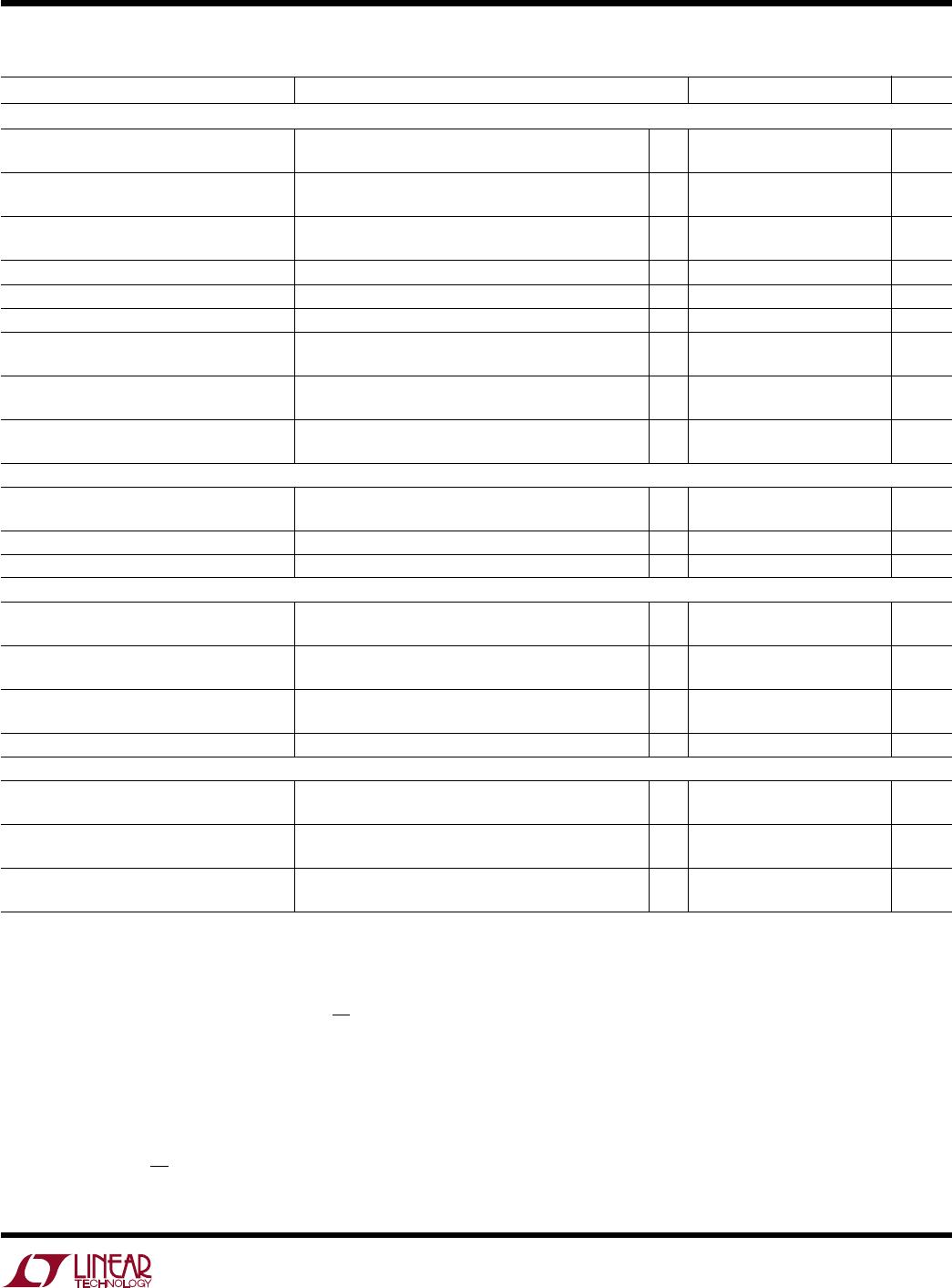
PARAMETER CONDITIONS MIN TYP MAX UNITS
Any Driver
Output Voltage Swing, Positive V
CC
= 5V, R
L
= 3k ● 5.0 6.5 V
V
CC
= 3.3V, R
L
= 3k 3.7 4.0 V
Output Voltage Swing, Negative V
CC
= 5V, R
L
= 3k ● –6.0 –5.0 V
V
CC
= 3.3V, R
L
= 3k –3.3 –2.7 V
Logic Input Voltage Level Input Low Level (V
OUT
= High) ● 1.4 0.8 V
Input High Level (V
OUT
= Low) ● 2.0 1.4 V
Logic Input Current 0.8V ≤ V
IN
≤ 2V ● 520 µA
Output Short-Circuit Current V
OUT
= 0V ±917 mA
Output Leakage Current Shutdown V
OUT
= ±30V (Note 5) ● 10 100 µA
Data Rate (Note 8) R
L
= 3k, C
L
= 2500pF 120 kBaud
R
L
= 3k, C
L
= 1000pF 250 kBaud
Slew Rate R
L
= 3k, C
L
= 51pF 15 30 V/µs
R
L
= 3k, C
L
= 2500pF 6 V/µs
Propagation Delay Output Transition t
HL
High to Low (Note 6) 0.6 1.3 µs
Output Transition t
LH
Low to High 0.5 1.3 µs
Any Receiver
Input Voltage Thresholds Input Low Threshold (V
OUT
= High) ● 0.8 1.3 V
Input High Threshold (V
OUT
= Low) ● 1.7 2.4 V
Hysteresis ● 0.1 0.4 1.0 V
Input Resistance V
IN
= ±10V 3 5 7 kΩ
Receivers 1 Through 4
Output Voltage Output Low, I
OUT
= –1.6mA ● 0.2 0.4 V
Output High, I
OUT
= 160µA (V
L
= 3.3V) ● 2.0 2.4 V
Output Short-Circuit Current Sinking Current, V
OUT
= V
CC
–20 –10 mA
Sourcing Current, V
OUT
= 0V 10 20 mA
Propagation Delay Output Transition t
HL
High to Low (Note 7) 250 600 ns
Output Transition t
LH
Low to High 350 600 ns
Output Leakage Current Shutdown (Note 5) 0 ≤ V
OUT
≤ V
CC
● 110 µA
Receiver 5 (Low Q-Current RX)
Output Voltage Output Low, I
OUT
= –500µA ● 0.2 0.4 V
Output High, I
OUT
= 160µA (V
L
= 3V) ● 2.0 2.4 V
Output Short-Circuit Current Sinking Current, V
OUT
= V
CC
–4 –2 mA
Sourcing Current, V
OUT
= 0V 2 4 mA
Propagation Delay Output Transition t
HL
High to Low (Note 7) 1 3 µs
Output Transition t
LH
Low to High 1 3 µs