BAV21W-G3-08

BAV19W-G, BAV20W-G, BAV21W-G
www.vishay.com
Vishay Semiconductors
Rev. 1.4, 22-Feb-18
1
Document Number: 85188
For technical questions within your region: DiodesAmericas@vishay.com
, DiodesAsia@vishay.com, DiodesEurope@vishay.com
THIS DOCUMENT IS SUBJECT TO CHANGE WITHOUT NOTICE. THE PRODUCTS DESCRIBED HEREIN AND THIS DOCUMENT
ARE SUBJECT TO SPECIFIC DISCLAIMERS, SET FORTH AT www.vishay.com/doc?91000
Small Signal Switching Diodes, High Voltage
DESIGN SUPPORT TOOLS
MECHANICAL DATA
Case: SOD-123
Weight: approx. 9.4 mg
Packaging codes / options:
18/10K per 13" reel (8 mm tape), 10K/box
08/3K per 7" reel (8 mm tape), 15K/box
FEATURES
Silicon epitaxial planar diodes
For general purpose
AEC-Q101 qualified available
(part number on request)
Base P/N-G3 - green, commercial grade
Material categorization:
for definitions of compliance please see
www.vishay.com/doc?99912
Note
(1)
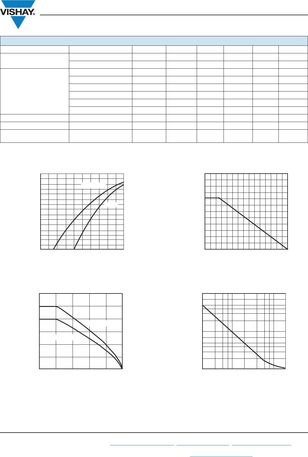
Valid provided that leads are kept at ambient temperature
click logo to get started
Available
Models
PARTS TABLE
PART
TYPE
DIFFERENTIATION
ORDERING CODE
TYPE
MARKING
CIRCUIT
CONFIGURATION
REMARKS
BAV19W-G V
R
= 100 V BAV19W-G3-08 or BAV19W-G3-18 AS Single Tape and reel
BAV20W-G V
R
= 150 V BAV20W-G3-08 or BAV20W-G3-18 AT Single Tape and reel
BAV21W-G V
R
= 200 V BAV21W-G3-08 or BAV21W-G3-18 AU Single Tape and reel
ABSOLUTE MAXIMUM RATINGS (T
amb
= 25 °C, unless otherwise specified)
PARAMETER TEST CONDITION PART SYMBOL VALUE UNIT
Continuous reverse voltage
BAV19W-G V
R
100 V
BAV20W-G V
R
150 V
BAV21W-G V
R
200 V
Repetitive peak reverse voltage
BAV19W-G V
RRM
120 V
BAV20W-G V
RRM
200 V
BAV21W-G V
RRM
250 V
DC forward current
(1)
I
F
250 mA
Rectified current (average) half
wave rectification with resist. load
(1)
I
F(AV)
200 mA
Repetitive peak forward current
(1)
f t 50 Hz I
FRM
625 mA
Surge forward current t < 1 s I
FSM
1A
Power dissipation
(1)
P
tot
410 mW
THERMAL CHARACTERISTICS (T
amb
= 25 °C, unless otherwise specified)
PARAMETER TEST CONDITION SYMBOL VALUE UNIT
Thermal resistance junction to ambient air
(1)
R
thJA
375 K/W
Junction temperature
(1)
T
j
150 °C
Storage temperature range
(1)
T
stg
-65 to +150 °C
Operating temperature range T
op
-55 to +150 °C
BAV19W-G, BAV20W-G, BAV21W-G
www.vishay.com
Vishay Semiconductors
Rev. 1.4, 22-Feb-18
2
Document Number: 85188
For technical questions within your region: DiodesAmericas@vishay.com
, DiodesAsia@vishay.com, DiodesEurope@vishay.com
THIS DOCUMENT IS SUBJECT TO CHANGE WITHOUT NOTICE. THE PRODUCTS DESCRIBED HEREIN AND THIS DOCUMENT
ARE SUBJECT TO SPECIFIC DISCLAIMERS, SET FORTH AT www.vishay.com/doc?91000
TYPICAL CHARACTERISTICS (T
amb
= 25 °C, unless otherwise specified)
Fig. 1 - Forward Current vs. Forward Voltage
Fig. 2 - Admissible Forward Current vs. Ambient Temperature
Fig. 3 - Admissible Power Dissipation vs. Ambient Temperature
Fig. 4 - Dynamic Forward Resistance vs. Forward Current
ELECTRICAL CHARACTERISTICS (T
amb
= 25 °C, unless otherwise specified)
PARAMETER TEST CONDITION PART SYMBOL MIN. TYP. MAX. UNIT
Forward voltage
I
F
= 100 mA V
F
1V
I
F
= 200 mA V
F
1250 mV
Leakage current
V
R
= 100 V BAV19W-G I
R
100 nA
V
R
= 100 V, T
j
= 100 °C BAV19W-G I
R
15 μA
V
R
= 150 V BAV20W-G I
R
100 nA
V
R
= 150 V, T
j
= 100 °C BAV20W-G I
R
15 μA
V
R
= 200 V BAV21W-G I
R
100 nA
V
R
= 200 V, T
j
= 100 °C BAV21W-G I
R
15 μA
Dynamic forward resistance I
F
= 10 mA r
f
5 :
Diode capacitance V
R
= 0, f = 1 MHz C
D
1.5 pF
Reverse recovery time
I
F
= 30 mA, I
R
= 30 mA,
i
R
= 3 mA, R
L
= 100 :
t
rr
50 ns
18858
1000
100
10
1
0.1
0.01
I - Forward Current (mA)
F
0 0.4 0.6 0.8 10.2
V
F
- Forward Voltage (V)
T
j
= 100 °C
25 °C
0.1
0.2
0.3
0
0 30 60 90 120 150
18859
T
amb
- Ambient Temperature (°C)
I , I - Admissible Forward Current (A)
OF
ICurrent (rectif.)
O
DC current I
F
21937
T
amb
- Ambient Temperature (°C)
P
tot
- Admissible Power Dissipation (mW)
0
100
200
300
400
500
600
0 20 40 60 80 100 120 140
r - Dynamic Forward Resistance
f
(Ω)
10
100
1
1 10010
18861
I
F
- Forward Current (mA)
BAV19W-G, BAV20W-G, BAV21W-G
www.vishay.com
Vishay Semiconductors
Rev. 1.4, 22-Feb-18
3
Document Number: 85188
For technical questions within your region: DiodesAmericas@vishay.com
, DiodesAsia@vishay.com, DiodesEurope@vishay.com
THIS DOCUMENT IS SUBJECT TO CHANGE WITHOUT NOTICE. THE PRODUCTS DESCRIBED HEREIN AND THIS DOCUMENT
ARE SUBJECT TO SPECIFIC DISCLAIMERS, SET FORTH AT www.vishay.com/doc?91000
Fig. 5 - Leakage Current vs. Junction Temperature Fig. 6 - Diodes Capacitance vs. Reverse Voltage
Fig. 7 - Non-Repetitive Peak Forward Current vs. Pulse Duration
Maximum Admissible Values of Square Pulses
0.1
18862-1
1
10
100
1000
0 40 80 120 160 200
I
R
(T
j
)/I
R
(25 °C) - Leakage Current
T
j
- Junction Temperature (°C)
Reverse Voltage
BAV19W-G V
R
= 100 V
BAV20W-G V
R
= 150 V
BAV21W-G V
R
= 200 V
21942
0.8
0.6
0.4
1.4
1.2
1.0
0.2
0
C - Diode Capacitance (pF)
D
V
R
- Reverse Voltage (V)
2.0
1.8
1.6
0 5 10 15 20 25 30 35
1
10
100
0.1
0.000001 0.00001 0.0001 0.001 0.01 0.1 1
t
p
- Test Pulse (s)
I
FSM
(A)
T
J
= 25 °C - Prior to Surge

BAV21W-G3-08

Mfr. #:
Manufacturer:
Vishay Semiconductors
Description:
Diodes - General Purpose, Power, Switching 250 Volt 200mA 50ns 1A IFSM
Lifecycle:
New from this manufacturer.
Delivery:
DHL FedEx Ups TNT EMS
Payment:
T/T Paypal Visa MoneyGram Western Union