LTC6362
9
6362fa
PIN FUNCTIONS
–IN (Pin 1): Inverting Input of Amplifier. Valid input range
is from V
–
to V
+
.
V
OCM
(Pin 2): Output Common Mode Reference Voltage.
The voltage on this pin sets the output common mode
voltage level. If left floating, an internal resistor divider
develops a default voltage of 2.5V with a 5V supply.
V
+
(Pin 3): Positive Power Supply. Operational supply
range is 2.8V to 5.25V when V
–
= 0V.
+OUT (Pin 4): Positive Output Pin. Output capable of
swinging rail-to-rail.
–OUT (Pin 5): Negative Output Pin. Output capable of
swinging rail-to-rail.
V
–
(Pin 6/Exposed Pad Pin 9): Negative Power Supply,
Typically 0V. Negative supply can be negative as long as
2.8V ≤ (V
+
– V
–
) ≤ 5.25V still holds.
SHDN (Pin 7): When SHDN is floating or directly tied to
V
+
the LTC6362 is in the normal (active) operating mode.
When the SHDN pin is connected to V
–
, the part is disabled
and draws approximately 70µA of supply current.
+IN (Pin 8): Noninverting Input of Amplifier. Valid input
range is from V
–
to V
+
.
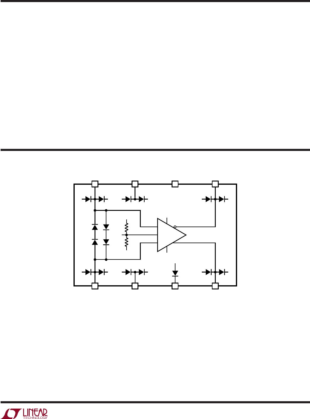
BLOCK DIAGRAM
–
+
8 567
1 432
V
+
V
+
340k
340k
V
OCM
V
–
V
–
+IN
–IN +OUT
6362 BD
V
+
V
–
V
OCM
–OUTV
–
SHDN
V
–
V
+
V
–
V
+
V
–
V
+
V
–
V
+
V
–
V
+
V
–
V
+